Method of operating a storage gate pixel

a storage gate and pixel technology, applied in the field of imaging devices, can solve the problems of poor sensitivity, low snr, and limited performance of conventional image sensors, and achieve the effects of effective reducing pixel noise, improving signal-to-noise ratio, and improving image quality

Active Publication Date: 2006-03-02
APTINA IMAGING CORP
View PDF11 Cites 81 Cited by
  • Summary
  • Abstract
  • Description
  • Claims
  • Application Information

AI Technical Summary

Benefits of technology

[0009] Exemplary embodiments of the invention provide devices and methods for effectively reducing pixel noise to achieve improved signal-to-noise ratio and thus, higher image quality in an imaging device.
[0010] According to one exemplary embodiment, a pixel with a storage gate is manufactured such that the storage gate does not have the same storage capacity as a photodiode. This configuration provides a greater fill factor for the pixel and a higher signal-to-noise ratio at low and mid-high noise levels.
[0011] In another exemplary embodiment, noise in an imager is reduced, and the signal-to-noise ratio of a pixel is enhanced, by storing photo-generated charge in a storage region of the pixel, determining whether the photo-generated charge exceeds the capacity of the storage region, and transferring a portion of the photo-generated charge to at least one diffusion region if the photo-generated charge exceeds the capacity of the storage region.
[0012] In yet another exemplary embodiment, noise in an imager is reduced, and the signal-to-noise ratio of a pixel is enhanced, by storing photo-generated charge in a storage region of the pixel, determining whether the photo-generated charge exceeds a predetermined threshold of the storage region, and transferring a portion of the photo-generated charge to at least one diffusion region if the photo-generated charge exceeds a predetermined threshold of the storage region.

Problems solved by technology

The performance of conventional image sensors, including CMOS image sensors, is often limited by a low signal-to-noise ratio (SNR) of the pixels, where SNR is a measure of the relative magnitude of a signal compared to the uncertainty or noise in the signal for each pixel.
Low SNR reduces image quality and may be caused, for example, by high fixed pattern noise (FPN), and other factors such as poor sensitivity and high dark current.
One common source of noise is pixel reset noise (or kT / C noise), which is often attributed to thermal noise uncertainty associated with a pixel reset level.
Because a pixel signal Vsig is measured relative to its reset level Vrst, high kT / C noise can interfere with the signal output from the pixel.
However, conventional image sensor circuits are usually not capable of effectively reducing noise over a range of signal intensities such as, for example, different levels of light intensity.
At high light levels, CDS techniques usually cannot reduce unwanted pixel noise in conventional image sensors.
Conventional image sensors are often not adequate for reducing all types of noise generated during image acquisition.

Method used


Image

  • Method of operating a storage gate pixel
  • Method of operating a storage gate pixel
  • Method of operating a storage gate pixel

Examples


Embodiment Construction

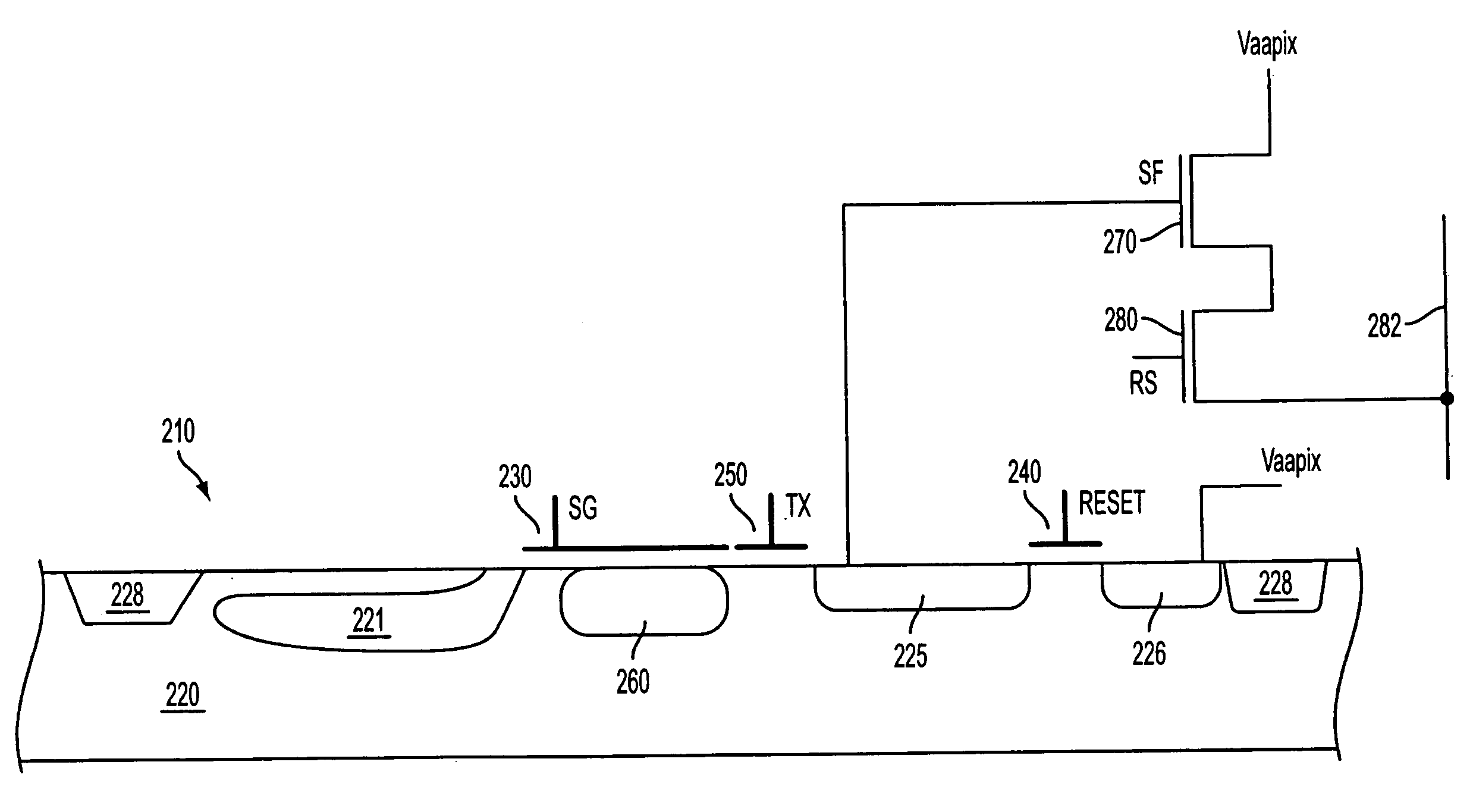
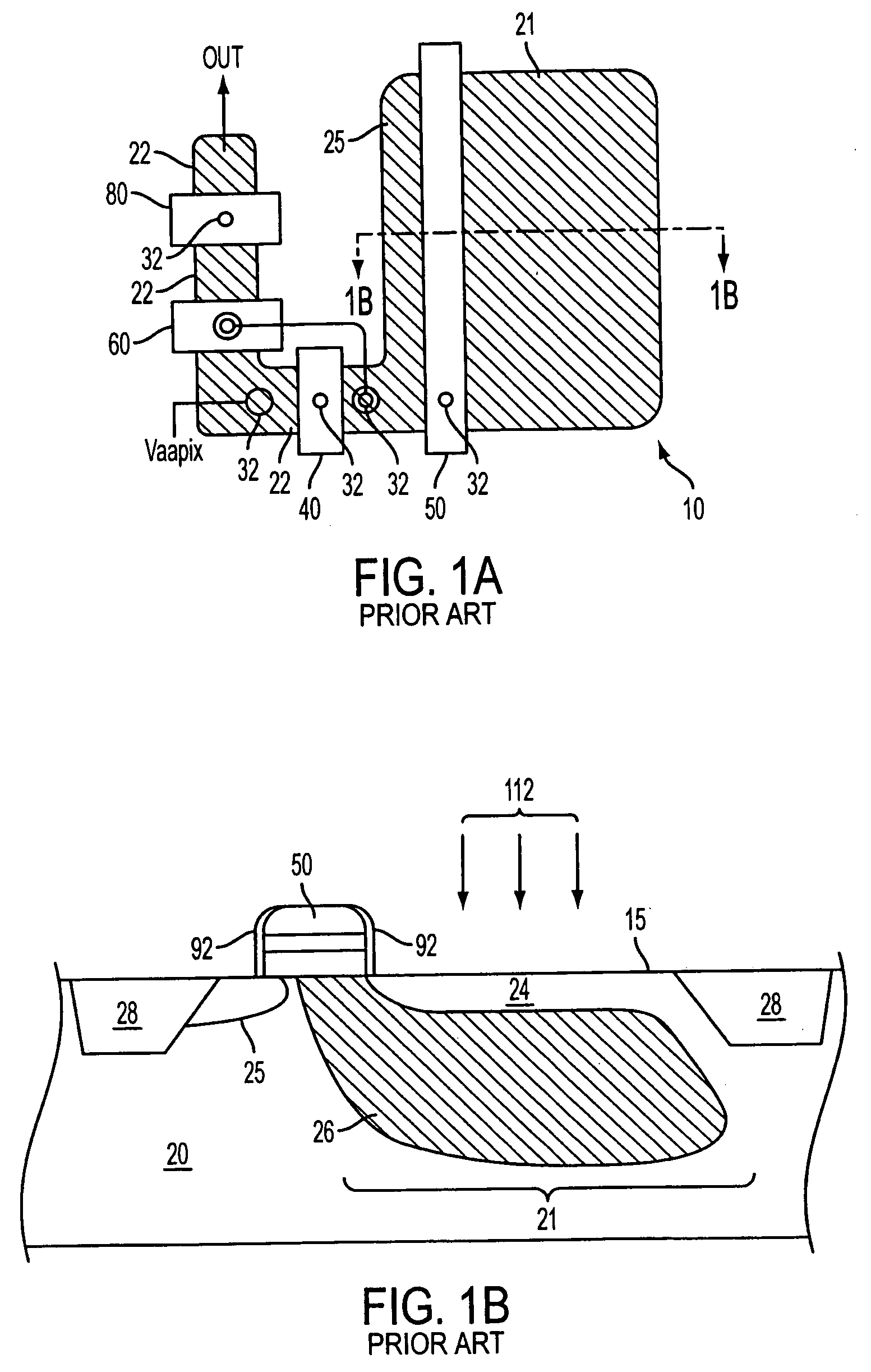
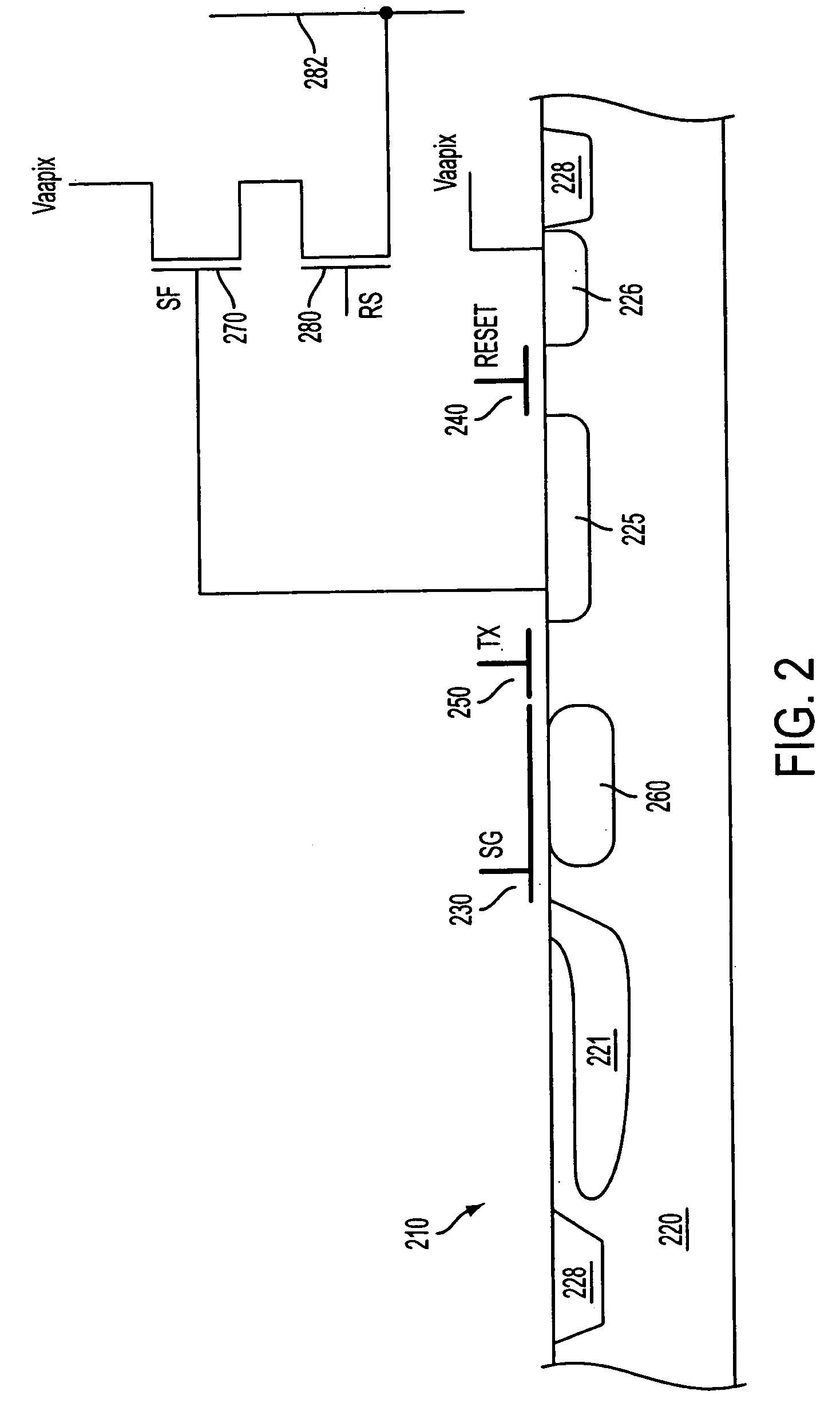
[0028] In the following detailed description, reference is made to various specific embodiments in which the invention may be practiced. These embodiments are described with sufficient detail to enable those skilled in the art to practice the invention, and it is to be understood that other embodiments may be employed, and that structural and logical changes may be made without departing from the spirit or scope of the present invention.

[0029] The terms “substrate” and “wafer” can be used interchangeably in the following description, and may include any semiconductor structure in or at a surface of which circuitry can be formed. The structure can include any of silicon, silicon-on insulator (SOI), silicon-on-sapphire (SOS), doped and undoped semiconductors, epitaxial layers of silicon supported by a base semiconductor foundation, and other semiconductor structures. The semiconductor need not be silicon-based. The semiconductor could be silicon-germanium, germanium, or gallium arsen...


PUM


Abstract

A storage gate pixel operates such that the storage gate is not required to have the same capacity as a photodiode of the pixel. This provides greater fill factor for the pixel and a higher signal to noise ratio.

Description

FIELD OF THE INVENTION [0001] The present invention relates generally to imaging devices and more particularly to a method of operating a storage gate pixel in an imaging device. BACKGROUND OF THE INVENTION [0002] An image sensor circuit includes a focal plane array of pixel cells, each one of the cells including either a photogate, photoconductor, or photodiode overlying a charge accumulation region within a substrate for accumulating photo-generated charge. In a conventional four transistor CMOS imager, the active elements of a pixel cell perform: (1) photon to charge conversion; (2) accumulation of image charge; (3) transfer of charge to a floating diffusion region accompanied by charge amplification; (4) resetting the floating diffusion region to a known state before the transfer of charge to it; (5) selection of a pixel for readout; and (6) output and amplification of a signal representing pixel charge. In a three transistor pixel cell the active elements of a pixel cell perfor...

Claims


Application Information

Patent Timeline
Patent Type & Authority Applications(United States)
IPC IPC(8): H04N3/14H04N5/335
CPCH01L27/14609H01L27/14654H04N5/365H04N5/363H04N5/3575H04N25/583H04N25/616H04N25/65H04N25/67
Inventor SHAH, JOEY
Owner APTINA IMAGING CORP
Why Eureka
Try Eureka