High speed semiconductor waveguide phase-shifter

a phase shifter and semiconductor technology, applied in multiplex communication, optical elements, instruments, etc., can solve the problems of low output intensity, and inability to achieve polarization independence and extensive integration of multiple channels and other components. , to achieve the effect of low voltage and power consumption, high speed and low optical loss

Active Publication Date: 2006-03-02
INFRARED NEWCO +2
View PDF8 Cites 19 Cited by
  • Summary
  • Abstract
  • Description
  • Claims
  • Application Information

AI Technical Summary

Benefits of technology

[0006] Advantageously, a phase-shifter device in accordance with the present invention can modulate the phase of an optical beam over a wide range, at high speeds, with low optical losses, and at low voltages and power consumption. Further advantageously, a device in accordance with the present invention can be readily designed to modulate orthogonally polarized beams of light at the same or different rates. The device of the present invention lends itself to integration with other components such as waveguides, splitters, combiners and integrated electronics and can be manufactured using practical, reliable and cost-effective manufacturing methods.

Problems solved by technology

When the copy of the light beam is subjected to a phase delay of π radians and combined with the original light beam, destructive interference occurs, yielding minimum output intensity.
Lithium niobate (LiNbO3) modulators can be fast and have reasonable voltage requirements, however, they are not polarization independent and do not lend themselves to integration of drive electronics and optical components.
Semiconductor modulators (InP or GaAs) can have a 40 GHz bandwidth; however, polarization independence and extensive integration of multiple channels and other components are not easily achieved with this technology.
Silicon modulators consisting of silicon waveguides embedded in silica allow extensive integration; however, designs to date have had a rather low phase change per unit voltage and length, requiring either a high operating voltage or a large device.

Method used


Image

  • High speed semiconductor waveguide phase-shifter
  • High speed semiconductor waveguide phase-shifter
  • High speed semiconductor waveguide phase-shifter

Examples


Embodiment Construction

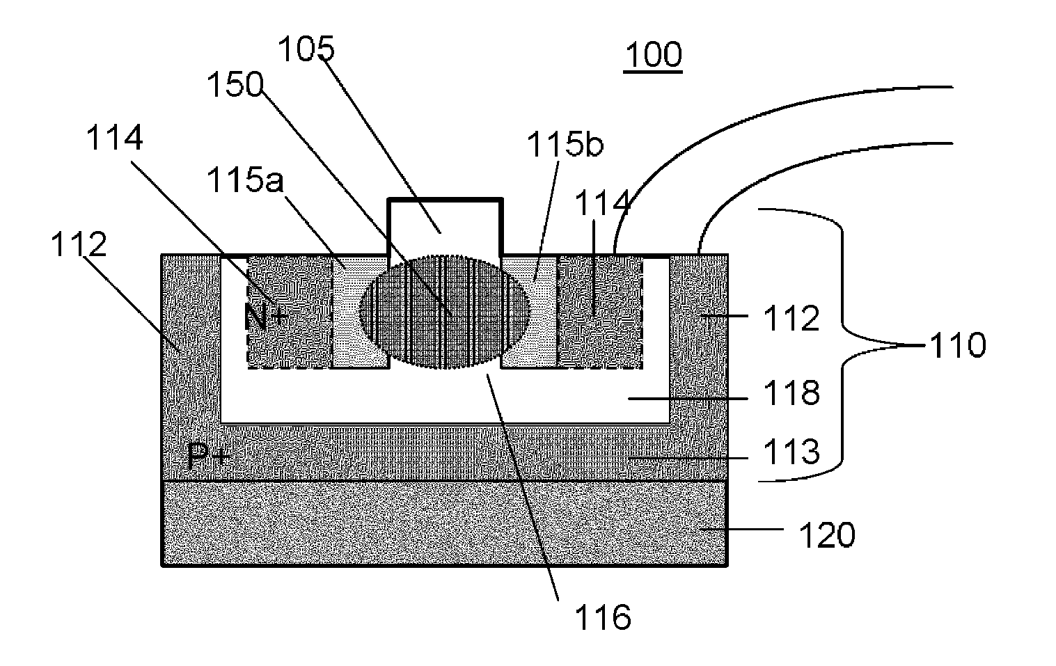
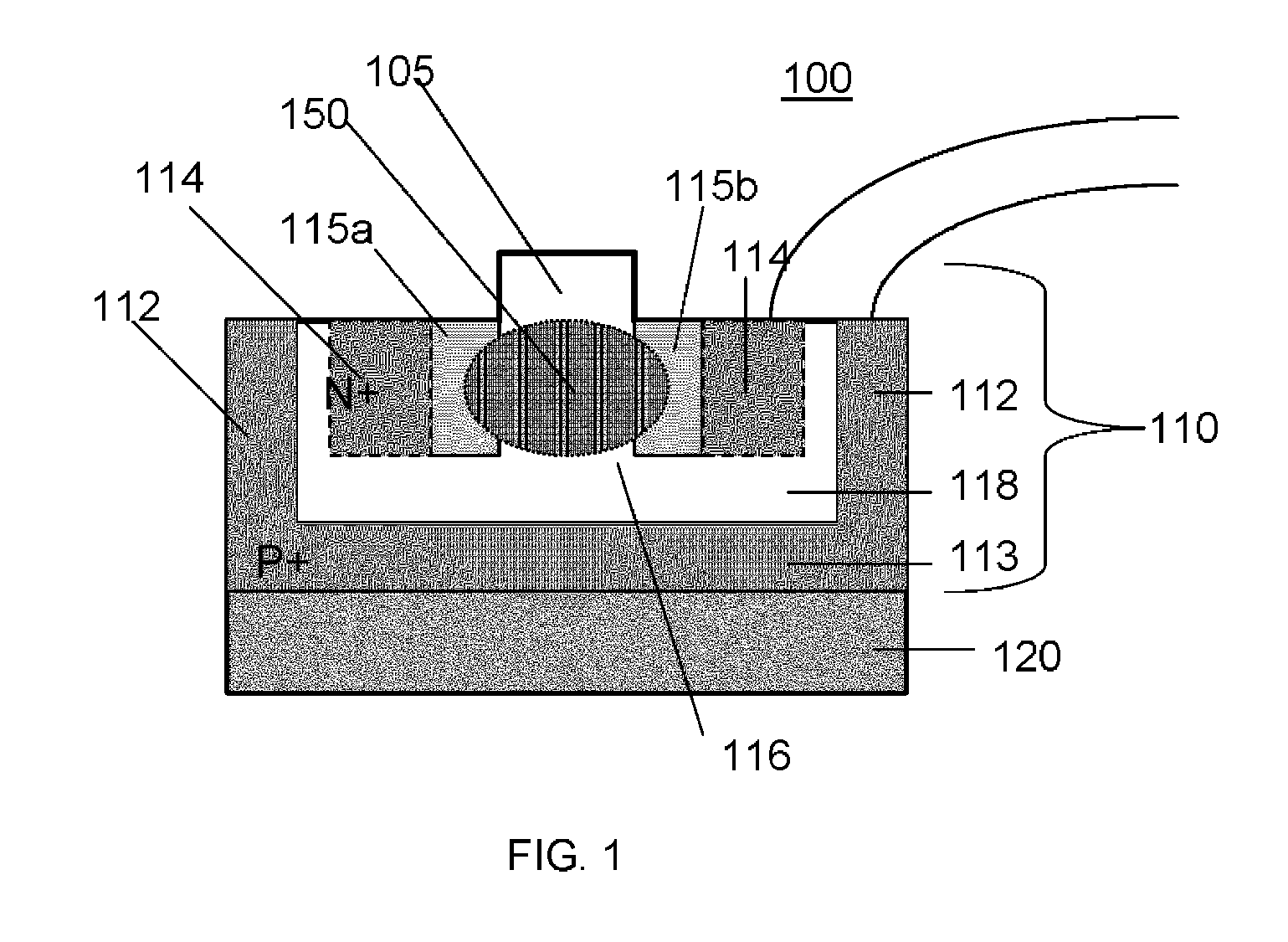
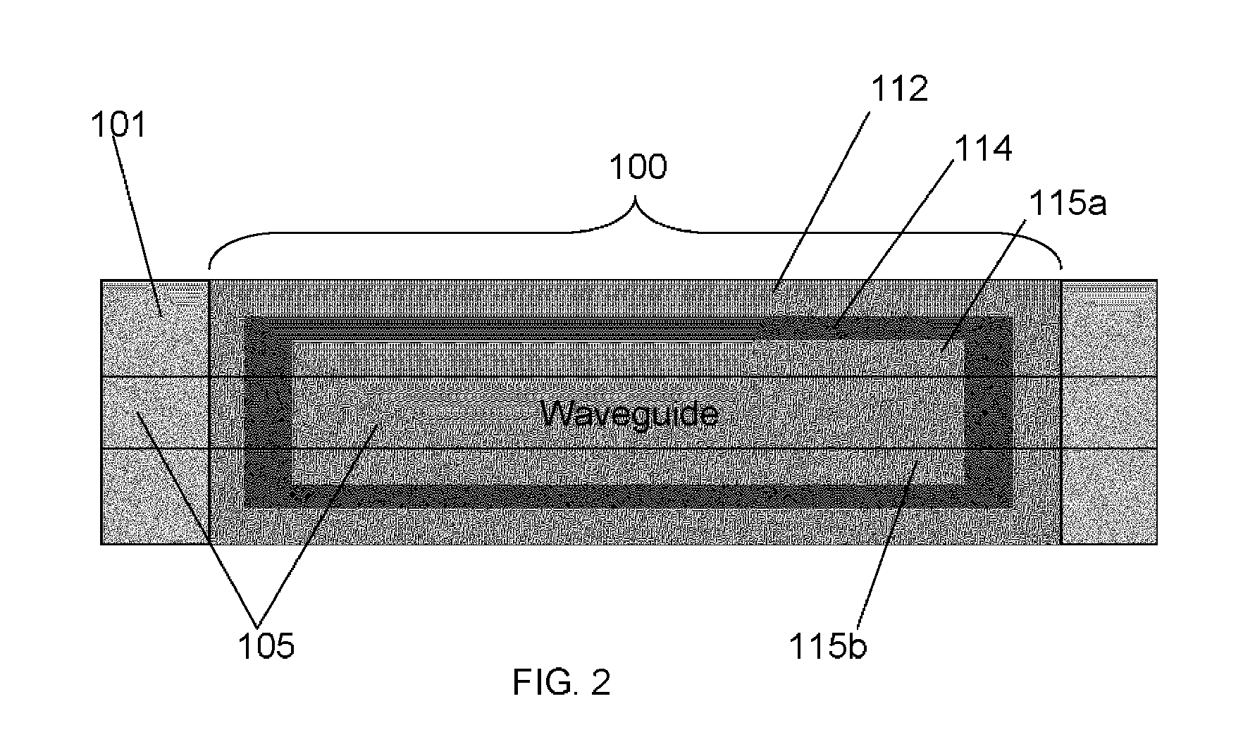
[0015] An exemplary embodiment of a phase shifting device 100 in accordance with the present invention is shown in cross section in FIG. 1 and in plan view in FIG. 2. The exemplary device shown uses a silicon rib waveguide 110 on a buffer layer 120 of silica (SiO2). A rib 105 is formed on the upper surface of the silicon rib waveguide 110. As shown in FIGS. 1 and 2, the silicon rib waveguide 110 has an outer region 112 and a base region 113 that are heavily P-type doped surrounding an inner region 114 that is heavily N-type doped. The heavily P-doped outer region 112 extends down to the heavily P-doped base region 113 whereas the heavily N-doped inner region 114 extends partially down into the silicon waveguide 110. Contacts are provided to the regions 112 and 114 to allow the application of a voltage there across, as described more fully below. To prevent leakage currents, the heavily doped regions 112 and 114 are preferably separated by a small gap as opposed to making direct cont...


PUM


Abstract

A semiconductor waveguide includes a section containing free charge, either electrons or holes, which can be steered into or removed from the path of the beam under the control of electrical signals. The mobile charges come from a potential well which may be either filled or depleted under electrical control. When the well is filled, the charges speed the beam propagation, introducing a phase change. When the well is emptied the beam propagates with extra delay. The phase shifter allows very high speed modulation of the beam using low voltage and low power electronics. The device can be created using standard silicon processing techniques, and integrated with other optical components such as splitters and combiners to create amplitude modulators, attenuators and other optical devices.

Description

CROSS-REFERENCE TO RELATED APPLICATIONS [0001] The present application is based on and claims priority from U.S. Provisional Patent Application No. 60 / 601,723, which was filed Aug. 16, 2004 and which is incorporated herein by reference in its entirety.FIELD OF THE INVENTION [0002] The present invention relates to the field of high-speed optical communications, and in particular, to phase shifter devices that can vary the phase of optical signals in accordance with electrical signals. BACKGROUND INFORMATION [0003] Data in optical communication is often encoded by modulation of the intensity of a beam of light. Such amplitude modulation can be achieved by combining a selectively delayed copy of a light beam with itself. When the copy of the light beam is subjected to a phase delay of π radians and combined with the original light beam, destructive interference occurs, yielding minimum output intensity. When the copy of the light beam is subjected to no phase delay, constructive interf...

Claims


Application Information

Patent Timeline
Patent Type & Authority Applications(United States)
IPC IPC(8): H04J14/00
CPCG02F2001/0153G02F1/025G02F1/0153H01L31/14
Inventor GILL, DOUGLASMMADSEN, CHRISTIKRAFFERTY, CONORS
Owner INFRARED NEWCO
Why Eureka
Try Eureka