Light emitting element and light emitting device using the same

a technology of light emitting elements and light emitting devices, applied in the direction of discharge tube luminescnet screens, organic semiconductor devices, natural mineral layered products, etc., can solve the problems of display failure, non-obtained light emission as an element, and problems on organic el elements, etc., to reduce inconvenience

Inactive Publication Date: 2006-03-02
SEMICON ENERGY LAB CO LTD
View PDF8 Cites 25 Cited by
  • Summary
  • Abstract
  • Description
  • Claims
  • Application Information

AI Technical Summary

Benefits of technology

[0015] In view of the foregoing problems, it is an object of the present invention to provide a light emitting element with reduced inconvenience due to dust or the like and a manufacturing method thereof.

Problems solved by technology

However, some problems on the organic EL element remain regardless of how the organic EL element is used.
One of the problems is display failure due to a manufacturing process.
Therefore, when current does not flow to a pixel or when current can not flow uniformly to a pixel by short circuit between two electrodes, light emission as an element is not obtained.
The former cause can be solved by selecting a material which is difficult to be crystallized; however, the latter cause can not be solved only by contriving the material since the cause is attributable to a manufacturing process.
In addition, when the concentration of an electric field further proceeds, the element is destroyed and short-circuited between two electrodes.
At this time, when the pixel is short-circuited by the above problem due to the process, the pixel is recognized as a black spot (hereinafter, referred to as a blind spot) on the screen, and the display quality is diminished.
However, in the case of considering the application for a display, minute dust generated during the process is hard to be completely removed since the process for manufacturing an active matrix type substrate is extremely complicated in particular.

Method used


Image

  • Light emitting element and light emitting device using the same
  • Light emitting element and light emitting device using the same
  • Light emitting element and light emitting device using the same

Examples


embodiment mode 1

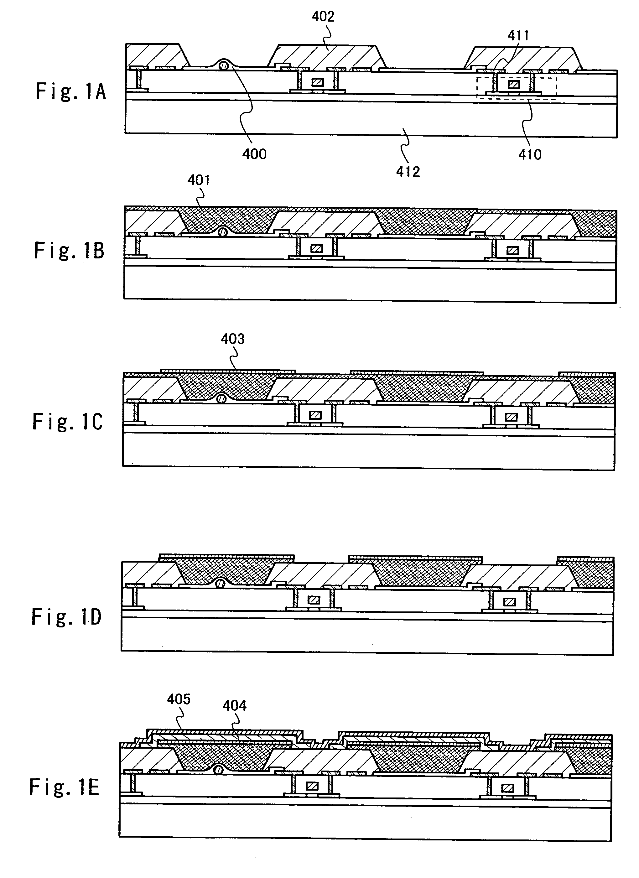
[0031] The case of forming an EL element over a substrate provided with a circuit for active matrix driving is described with reference to FIGS. 1A to 1E; however, the invention is not limited to the mode of a substrate, and a substrate provided with a circuit for passive matrix driving or a substrate having only a single pixel may be used.

[0032] First, an organic EL element is required to extract light; therefore, at least one of an anode and a cathode is required to be transparent. Hereinafter, a light emitting element in which light can be extracted from an anode side by forming a transparent anode over a substrate is explained. However, the invention is not limited to this structure. For example, the invention can be applied to a structure in which only a cathode is transparent or a structure in which both of an anode and a cathode are transparent to obtain light emission from the above and below the element.

[0033] Next, the light emitting element according to the invention is...

embodiment mode 2

[0050] A light emitting element of the present invention has less failure due to dust or the like; therefore, a light emitting device with no display failure or the like due to inconvenience of a light emitting element can be obtained using the light emitting element of the invention for a pixel or the like.

[0051] In this embodiment mode, the circuit configuration and driving method of a light emitting device including the light emitting element of the invention and having a display function are explained with reference to FIGS. 4 to 7.

[0052]FIG. 4 is a schematic top view of a light emitting device to which the invention is applied. In FIG. 4, a pixel portion 6511, a source signal line driver circuit 6512, a writing gate signal line driver circuit 6513, and an erasing gate signal line driver circuit 6514 are provided over a substrate 6500. The source signal line driver circuit 6512, the writing gate signal line driver circuit 6513, and the erasing gate signal line driver circuit 6...

embodiment mode 3

[0072] A light emitting device including a light emitting element according to the present invention can display a favorable image; therefore, an electronic device which can provide an excellent image can be obtained by applying the light emitting device according to the invention to the display portion of an electronic device.

[0073] One example of the electronic device mounted with the light emitting device to which the invention is applied is shown in FIGS. 8A to 8C.

[0074]FIG. 8A is a personal computer manufactured by applying the invention, which includes a main body 5521, a casing 5522, a display portion 5523, a keyboard 5524, and the like. The personal computer can be completed by incorporating the light emitting device having the light emitting element according to the invention as the display portion.

[0075]FIG. 8B is a telephone manufactured by applying the invention, which includes a main body 5552, a display portion 5551, an audio output portion 5554, an audio input port...


PUM

PropertyMeasurementUnit
thicknessaaaaaaaaaa
thicknessaaaaaaaaaa
thicknessaaaaaaaaaa

Abstract

It is an object of the present invention to provide a light emitting element with reduced inconvenience due to dust or the like and a manufacturing method thereof. One feature of the invention is a light emitting element having a first layer provided so as to be in contact with a first electrode, and a second layer provided so as to be in contact with the first layer, between the first electrode and a second electrode. A light emitting layer exists between the second layer and the second electrode. The first electrode, the second electrode, the first layer, the second layer, and the light emitting layer are stacked so that the first layer is formed in advance compared with the second layer. Here, the first layer is a layer containing an organic compound. Especially, an organic compound having conductivity is preferable among organic compounds. Alternatively, the second layer is a layer containing an inorganic compound. In particular, an inorganic compound having hole transport property is preferable among inorganic compounds.

Description

BACKGROUND OF THE INVENTION [0001] 1. Field of the Invention [0002] The present invention relates to a technical field in respect of a light emitting device provided with an element having a structure interposing a thin film which emits light by a phenomenon called electroluminescence (hereinafter, referred to as “EL”) between an anode and a cathode over a substrate. [0003] 2. Description of the Related Art [0004] An EL element is an element which emits light by forming a thin film or a crystal containing an organic compound or an inorganic compound between a cathode and an anode and by flowing current between the cathode and anode. In recent years, an EL element in which a thin film (hereinafter, referred to as an organic thin film) chiefly containing an organic compound as a main constituent is located between a cathode and an anode, namely an organic EL element, has been actively developed. [0005] The organic EL element is expected to be applied to various fields and is considere...

Claims


Application Information

Patent Timeline
Patent Type & Authority Applications(United States)
IPC IPC(8): H05B33/12H05B33/10
CPCH01L51/0037H01L51/0059H01L51/0081H01L2251/558H01L51/0087H01L51/5048H01L51/5088H01L51/0085H10K85/1135H10K85/631H10K85/346H10K85/324H10K85/342H10K50/14H10K50/17H10K2102/351
Inventor NOMURA, RYOJISUZUKI, TSUNENORISEO, SATOSHI
Owner SEMICON ENERGY LAB CO LTD
Why Eureka
Try Eureka