Ferroelectric memory and its manufacturing method

a manufacturing method and technology of ferroelectric memory, applied in the direction of basic electric elements, electrical apparatus, semiconductor devices, etc., can solve the problems of lowering reliability and stability of manufacturing process, and achieve the effect of simplifying the manufacturing process

Active Publication Date: 2006-03-02
FUJITSU SEMICON MEMORY SOLUTION LTD
View PDF2 Cites 14 Cited by
  • Summary
  • Abstract
  • Description
  • Claims
  • Application Information

AI Technical Summary

Benefits of technology

[0037] By this, the laminated body that becomes the ferroelectric capacitor and the adhesion layer can be patterned in the same process, such that the manufacturing process can be simplified.

Problems solved by technology

However, in this case, a recess (concave section), which is caused by a difference in the polishing rate between the conductive layer and the surrounding dielectric layer, is generated in the conductive layer at the contact hole.
If the recess is left remained, the ferroelectric capacitor cannot be formed on a flat surface, so that the stability in the manufacturing process may be damaged, and the reliability may possibly be lowered.

Method used


Image

  • Ferroelectric memory and its manufacturing method
  • Ferroelectric memory and its manufacturing method
  • Ferroelectric memory and its manufacturing method

Examples


first embodiment

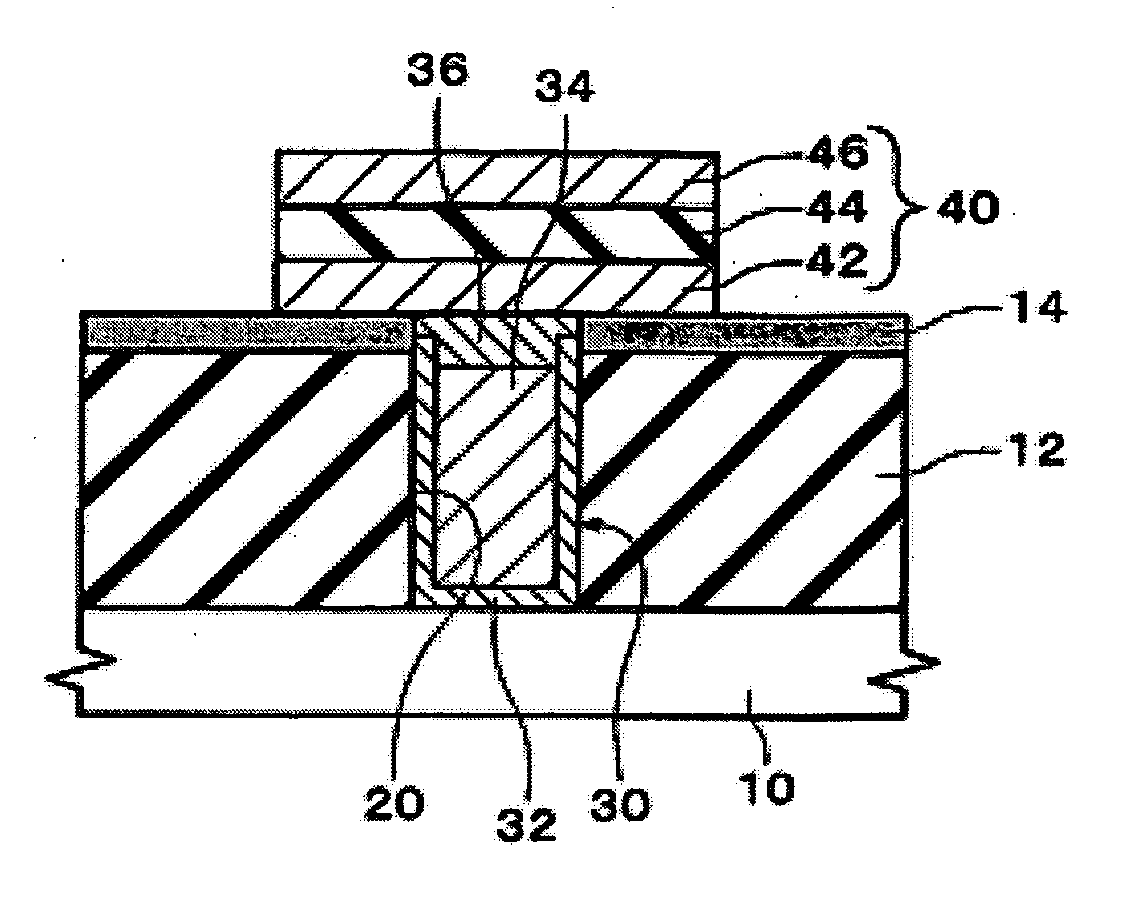
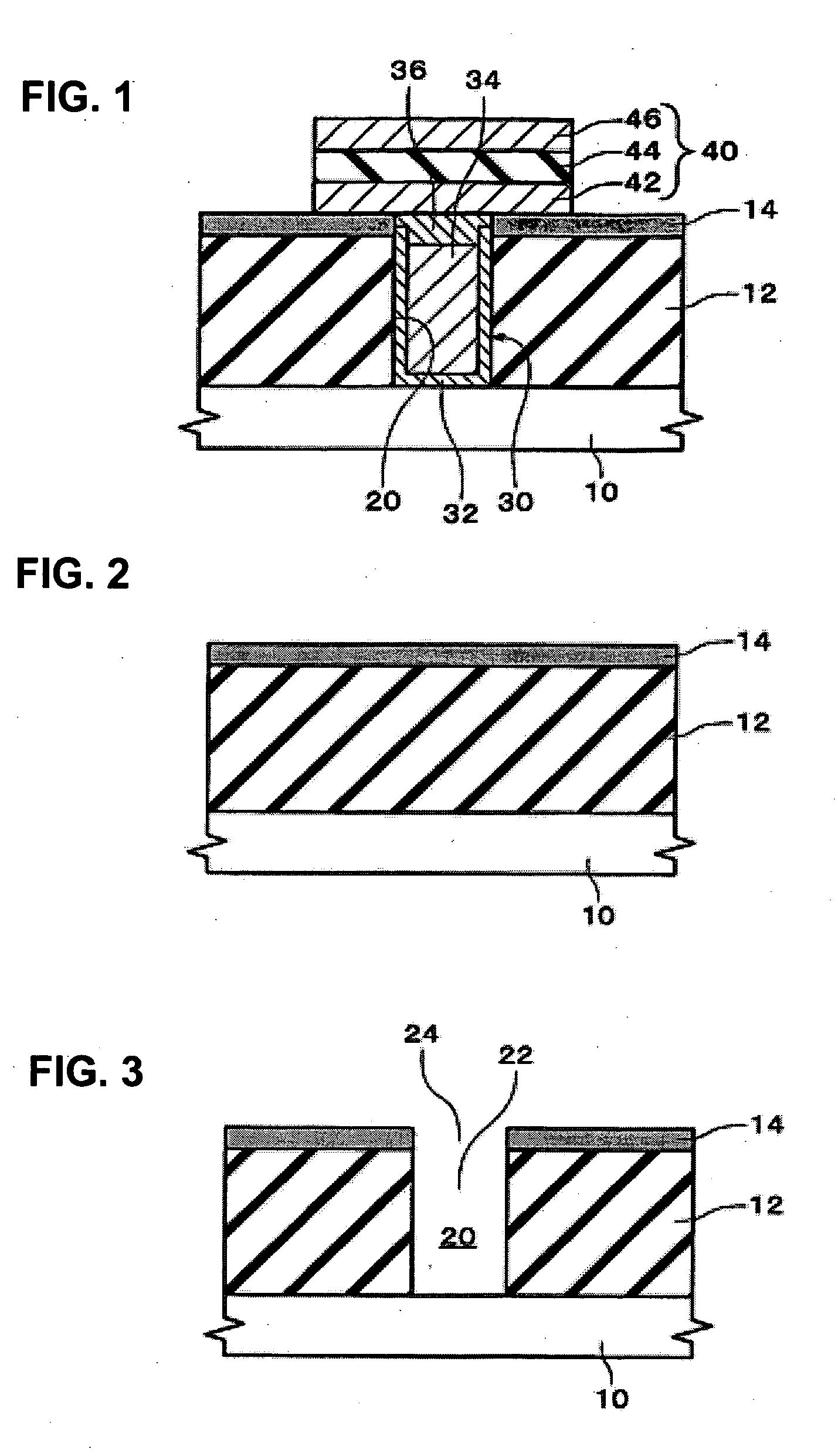
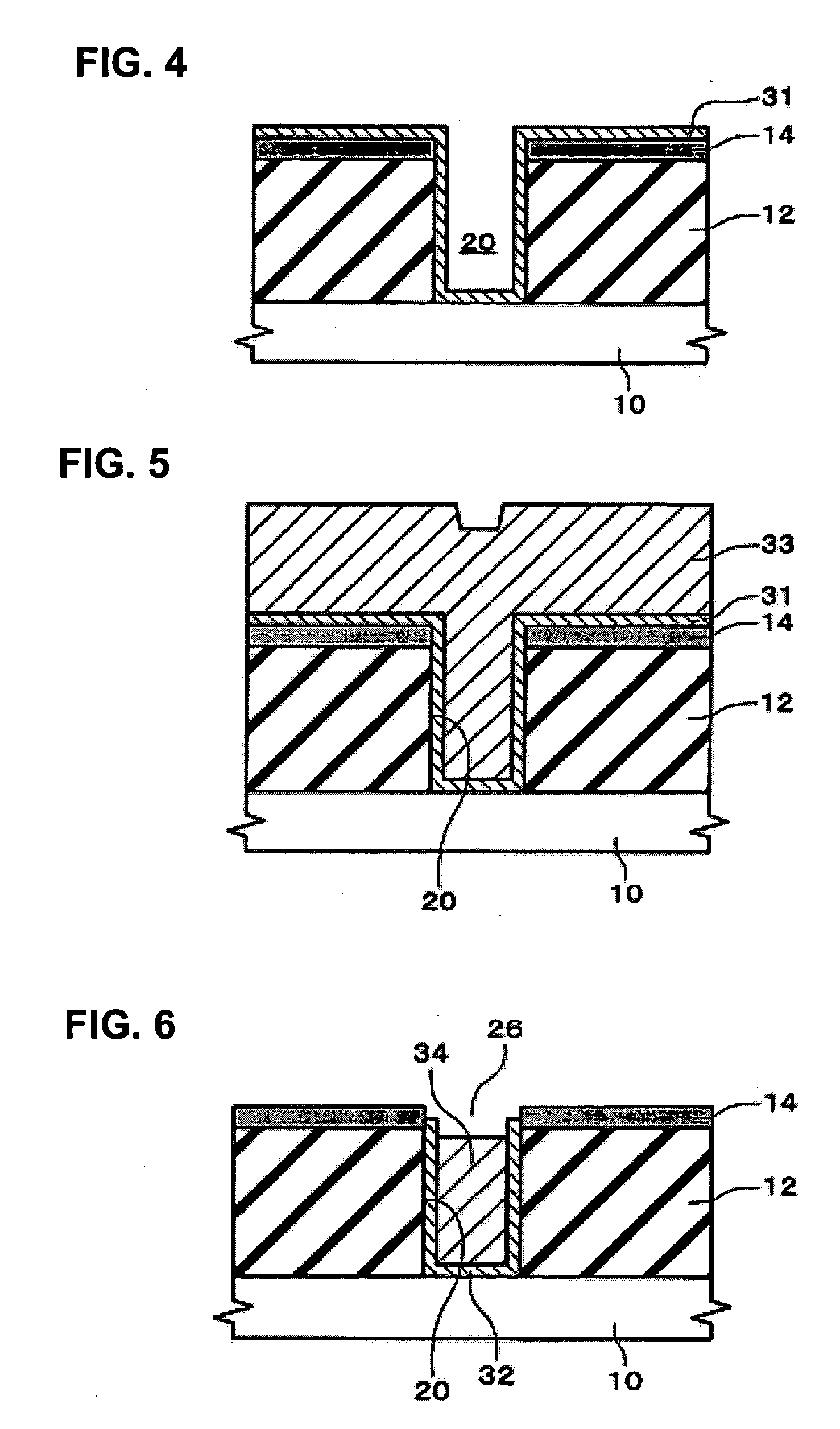
[0051]FIG. 1 is a view schematically showing a ferroelectric memory in accordance with a first embodiment of the present invention.

[0052] The ferroelectric memory in accordance with the present embodiment includes a base member 10, first and second dielectric layers 12 and 14, a contact hole 20, a contact section 30, and a ferroelectric capacitor 40.

[0053] The base member 10 is a semiconductor substrate (for example, a silicon substrate). A plurality of transistors (not shown) is formed in the base member 10. Each transistor includes an impurity region that becomes to be a source region or a drain region, a gate dielectric layer, and a gate electrode. An element isolation region (not shown) is formed between adjacent transistors, to provide electrical insulation between the transistors. The ferroelectric memory in accordance with the present embodiment is, for example, a 1T1C type with a stacked structure.

[0054] The first dielectric layer 12 is formed on the base member 10. When ...

second embodiment

[0082]FIG. 10 is a view schematically showing a ferroelectric memory in accordance with a second embodiment of the present invention.

[0083] The ferroelectric memory in accordance with the present embodiment includes the composition of the ferroelectric memory described above, and further includes an adhesion layer 50.

[0084] The adhesion layer 50 is formed between a lower electrode 42 and a barrier layer 36 (a contact section 30). As shown in FIG. 10, the lower electrode 42 may be formed on one of surfaces of the adhesion layer 50, and the barrier layer 36 may be formed on the other surface. Also, the adhesion layer 50 is formed in a region including the lower electrode 42. In other words, in a plan view viewed in a direction orthogonal to the surface of the base member 10, a plane area of the adhesion layer 50 includes at least a plane area of the lower electrode 42. For example, the plane area of the adhesion layer 50 may generally match with the plane area of the lower electrode...


PUM

PropertyMeasurementUnit
ferroelectricaaaaaaaaaa
adhesionaaaaaaaaaa
conductiveaaaaaaaaaa

Abstract

A ferroelectric memory includes a base member, a first dielectric layer formed above the base member, a second dielectric layer formed above the first dielectric layer, a contact hole that penetrates the first and second dielectric layers, a plug formed in the contact hole, and a barrier layer formed above the plug, and a ferroelectric capacitor formed from a lower electrode, a ferroelectric layer and an upper electrode successively laminated in a region including above the plug. The second dielectric layer has a property that is more difficult to be polished than the plug and the first dielectric layer.

Description

RELATED APPLICATIONS [0001] This application claims priority to Japanese Patent Application No. 2004-245361 filed Aug. 25, 2004 which is hereby expressly incorporated by reference herein in its entirety. BACKGROUND [0002] 1. Technical Field [0003] The present invention relates to ferroelectric memories and methods for manufacturing the same. [0004] 2. Related Art [0005] For ferroelectric memories, the structure in which a ferroelectric capacitor is stacked on a selection transistor is known. A dielectric layer is provided between the ferroelectric capacitor and the selection transistor, and an electrical connection between them is made by a plug embedded in a contact hole in the dielectric layer. The plug is formed by forming a film of conductive layer that is a plug material inside the contact hole and on the dielectric layer, and the entire conductive layer is polished by using a chemical mechanical polishing (CMP) method or the like. However, in this case, a recess (concave secti...

Claims


Application Information

Patent Timeline
Patent Type & Authority Applications(United States)
IPC IPC(8): H01L21/00
CPCH01L27/11507H01L27/11502H10B53/30H10B53/00
Inventor UEDA, MAMORUMASUDA, KAZUHIROFUKADA, SHINICHI
Owner FUJITSU SEMICON MEMORY SOLUTION LTD
Why Eureka
Try Eureka