Epitaxial substrate and semiconductor element

a technology of semiconductor elements and substrates, applied in the direction of basic electric elements, semiconductor devices, electrical apparatus, etc., can solve the problems of insufficient reverse blocking voltage of pin diodes in irokawa paper, inability to produce devices on low dislocation areas, complex device structure in this paper, etc., to achieve the effect of improving reverse breakdown

Active Publication Date: 2006-03-02
SUMITOMO ELECTRIC IND LTD
View PDF2 Cites 32 Cited by
  • Summary
  • Abstract
  • Description
  • Claims
  • Application Information

AI Technical Summary

Benefits of technology

[0019] With this semiconductor element, the dislocation in the epitaxial layer is reduced, the reverse leakage current is reduced, and the reverse breakdown improves.
[0039] As described above, with the present invention, a group III nitride element with a structure that can improve reverse breakdown is provided. Also, an epitaxial substrate for this semiconductor element is provided.

Problems solved by technology

However, the device structure in this paper is complex and production of the device on the low-dislocation area is not practical.
The reverse blocking voltage of the PIN diode in the Irokawa paper is also not high enough.
However, if the thickness of the epitaxial layer is not adequate for the carrier concentration, causing depletion of the entire thickness of the epitaxial layer before the field intensity at the junction reaches the critical value (punch-through), the field intensity at the junction will reach the critical value earlier so that breakdown takes place at a lower voltage compared to the ideal case described above.
Also, since the depletion layer extends to the boundary surface between the epitaxial layer and the substrate, leaked current caused by imperfections in the boundary surface can reduce the reverse characteristics of the leakage current, possibly lowering the breakdown voltage.

Method used


Image

  • Epitaxial substrate and semiconductor element
  • Epitaxial substrate and semiconductor element
  • Epitaxial substrate and semiconductor element

Examples


first embodiment

(First Embodiment)

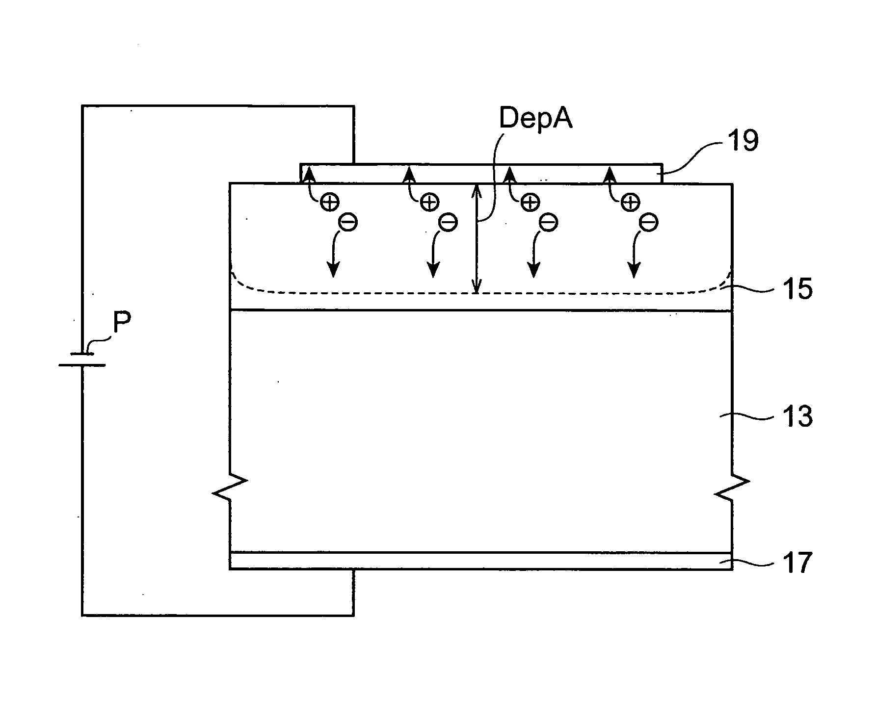
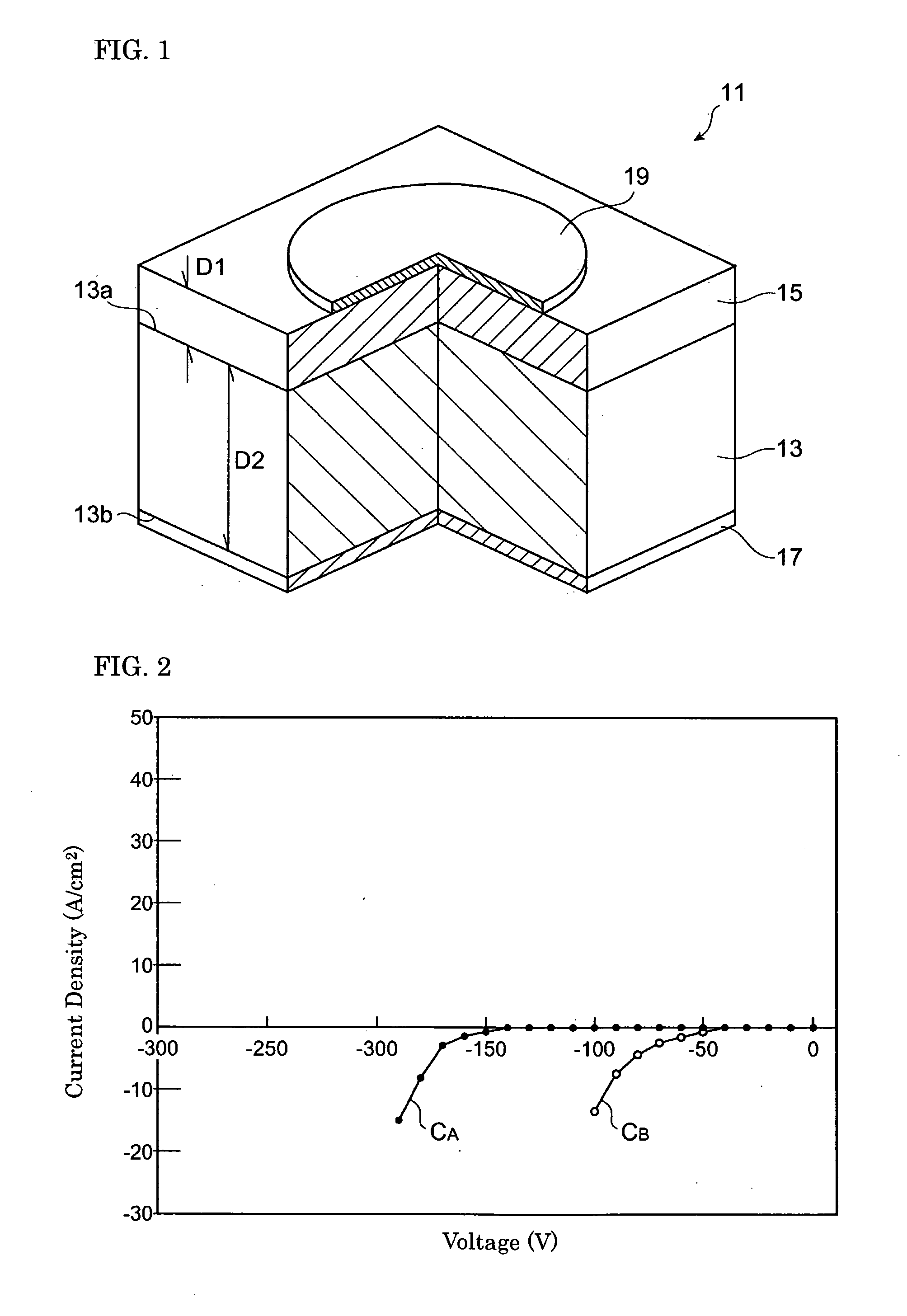
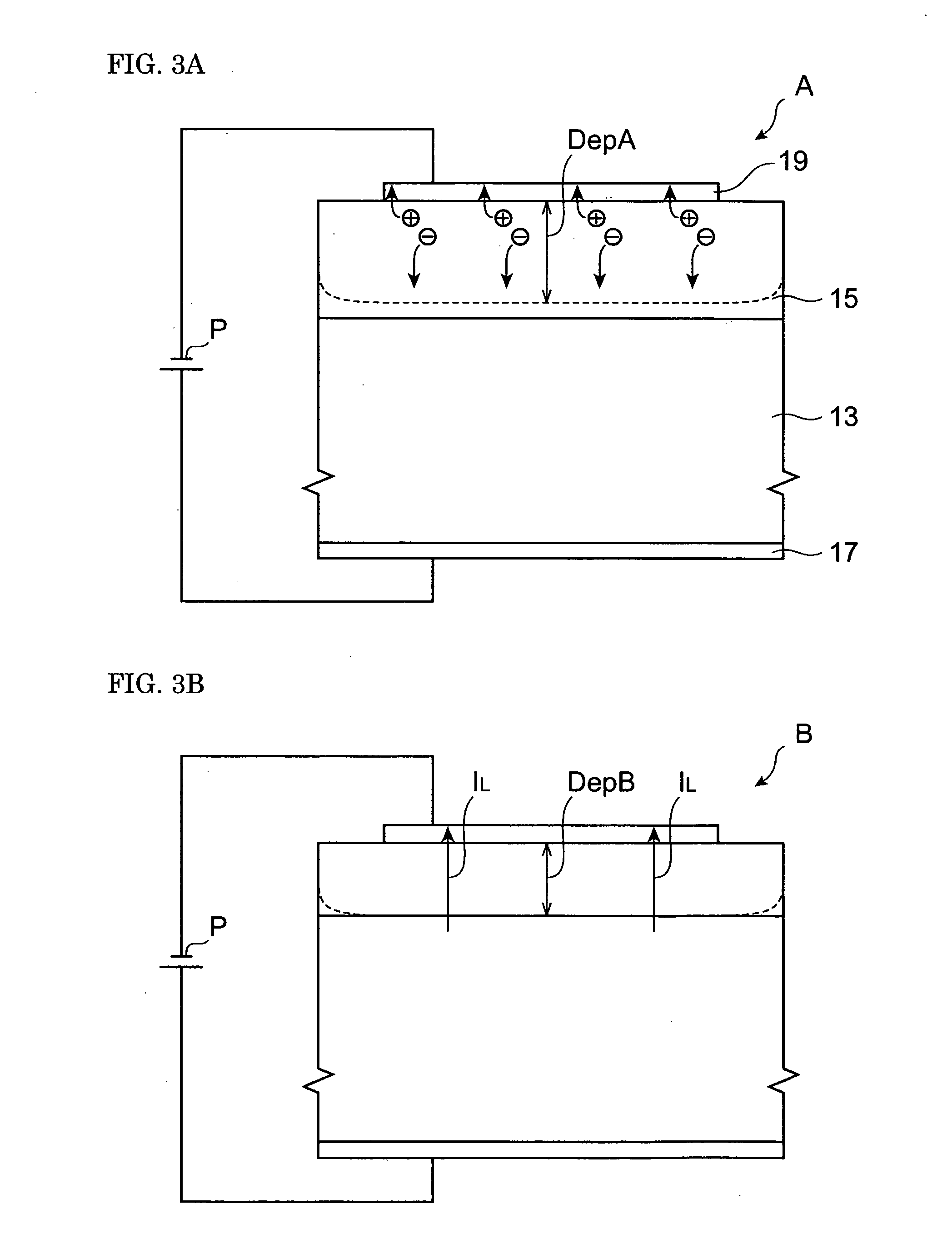
[0052]FIG. 1 shows a group III nitride semiconductor element according to a first embodiment of the present invention. This semiconductor element is a Schottky diode 11. The Schottky diode 11 is equipped with a gallium nitride support base 13, a gallium nitride epitaxial layer 15, an Ohmic electrode 17, and a Schottky electrode 19. The gallium nitride support base 13, which includes a first surface 13a and a second surface 13b opposite from the first surface, has a carrier concentration of over 1×1018 cm−3. The gallium nitride epitaxial layer 15 is disposed on the first surface 13a. The Ohmic electrode 17 is disposed on the second surface 13b. The Schottky electrode 19 is disposed on the gallium nitride epitaxial layer 15. The thickness D1 of the gallium nitride epitaxial layer 15 is 5 microns or more and 1000 microns or less. Also, the carrier concentration of the gallium nitride epitaxial layer 15 is 1×1014 cm−3 or more and 1×1017 cm−3 or less. With the carrier c...

first working example

[0055] An HPVE-produced (0001) face GaN free-standing substrate is prepared. A Schottky diode is produced using the procedure described below. The carrier concentration of an n-type conductor GaN free-standing substrate is 3×1018 cm−3, and the thickness is 400 microns. The average dislocation density in this substrate is 5×106 cm−2. An n-type conductor epitaxial film having a carrier concentration of 5×1015 cm−3 and a thickness of 20 microns is grown using HVPE on the GaN free-standing substrate, thus forming an epitaxial substrate (hereinafter referred to as sample A). An Ohmic electrode is formed on the back side of the substrate, and a Schottky electrode is formed on the epitaxial film. The Ohmic electrode is formed on the entire back surface of the substrate after organic cleaning is performed. To form the Ohmic electrode, Ti / Al / Ti / Au (20 nm / 100 nm / 20 nm / 300 nm) are formed using EB vapor deposition. After the Ohmic electrode film is formed, it is alloyed for approximately 1 minu...

second working example

[0058] An HPVE-produced (0001) face GaN free-standing substrate is prepared. The carrier concentration of the n-type conductor GaN free-standing substrate is 3×1018 cm−3, and the thickness is 400 microns. The average dislocation density in this substrate is 5×105 cm−2. An n-type conductor epitaxial film having a carrier concentration of 5×1015 cm−3 and a thickness of 20 microns is grown using HVPE on the GaN free-standing substrate, thus forming an epitaxial substrate (sample C). The process used in the first working example is used on this epitaxial substrate to produce a Schottky diode.

[0059]FIG. 4 is a drawing showing the I-V characteristics of sample A and sample C. In FIG. 4, the characteristic curve CA indicates the characteristics of sample A, and a characteristic curve Cc indicates the characteristics of sample C. The average dislocation density in the GaN free-standing substrate of sample A is 5×106 cm−2, while the average dislocation density in the GaN free-standing subst...


PUM

PropertyMeasurementUnit
carrier concentrationaaaaaaaaaa
thicknessaaaaaaaaaa
thicknessaaaaaaaaaa

Abstract

In a Schottky diode 11, a gallium nitride support base 13 includes a first surface 13a and a second surface 13b opposite from the first surface and has a carrier concentration exceeding 1×1018 cm−3. A gallium nitride epitaxial layer 15 is disposed on the first surface 13a. An Ohmic electrode 17 is disposed on the second surface 13b. The Schottky electrode 19 is disposed on the gallium nitride epitaxial layer 15. A thickness D1 of the gallium nitride epitaxial layer 15 is at least 5 microns and no more than 1000 microns. Also, the carrier density of the gallium nitride epitaxial layer 15 is at least 1×1014 cm−3 and no more than 1×1017 cm−3.

Description

INCORPORATION BY REFERENCE [0001] The present application claims priority under 35 U.S.C. §119 to Japanese Patent Application No. 2004-254815 filed on Sep. 1, 2004 in the Japanese language, which is hereby incorporated by reference in its entirety. BACKGROUND OF THE INVENTION [0002] 1. Field of the Invention [0003] The present invention relates to an epitaxial substrate and a semiconductor element. [0004] 2. Description of the Background Art [0005] Y. Irokawa, et. al., Appl. Phys. Lett., Vol. 83, No. 11, 15 Sep. 2003 describes a PIN diode. The PIN diode is equipped with an epitaxial layer grown on a GaN free-standing substrate. The thick film used as the GaN free standing substrate is grown using the hydride vapor phase epitaxy (HVPE) method on an Al2O3 substrate. A laser is applied to this thick film to separate it from the Al2O3 substrate to form the GaN free-standing substrate. On this GaN free-standing substrate, metal-organic vapor phase growth epitaxy is used to grow an undope...

Claims


Application Information

Patent Timeline
Patent Type & Authority Applications(United States)
IPC IPC(8): H01L21/00H01L21/20H01L21/329H01L21/336H01L29/12H01L29/47H01L29/78H01L29/861H01L29/868H01L29/872
CPCH01L29/045H01L29/2003H01L29/41741H01L29/872H01L29/7802H01L29/861H01L29/4238
Inventor KIYAMA, MAKOTOOKAHISA, TAKUJISAKURADA, TAKASHI
Owner SUMITOMO ELECTRIC IND LTD
Why Eureka
Try Eureka