
Vertical wrap-around-gate field-effect-transistor for high density, low voltage logic and memory array

a field effect transistor and vertical wrap technology, applied in the field of transistors, can solve the problems of increasing manufacturing costs, increasing the cost of photolithographic equipment, and increasing the cost of capital equipment,

Active Publication Date: 2006-03-02
MICRON TECH INC
View PDF33 Cites 139 Cited by
  • Summary
  • Abstract
  • Description
  • Claims
  • Application Information

AI Technical Summary

Problems solved by technology

As the industry standard approaches smaller and smaller scaled devices, problems with further advancement are presented and it becomes more difficult to produce sub-micron devices that can perform as desired.
These additional steps add significantly to manufacturing costs.
High capital costs are associated with photolithographic equipment and more complex photo processing, in terms of more photo process steps per level, more equipment, and the use of expensive ultra clean room floor space.
Furthermore, the smallest separation between semiconductor structures using known patterning methods is subject to the physical limitations of how thin a distinguishable line or gap can be formed in a photoresist layer by patterning with a reticle.
Thus, use of such photolithographic patterning methods places an upper limit to the highest achievable density of a semiconductor device.
In addition, defect density is inevitably increased with each additional photomasking layer, which thereby compromises yield and reliability.

Method used


Image

  • Vertical wrap-around-gate field-effect-transistor for high density, low voltage logic and memory array
  • Vertical wrap-around-gate field-effect-transistor for high density, low voltage logic and memory array
  • Vertical wrap-around-gate field-effect-transistor for high density, low voltage logic and memory array

Examples


Embodiment Construction

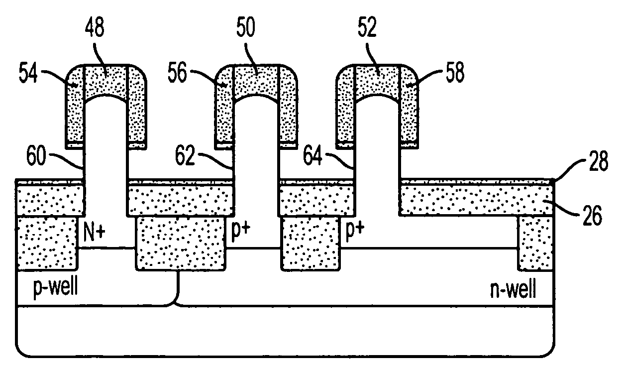
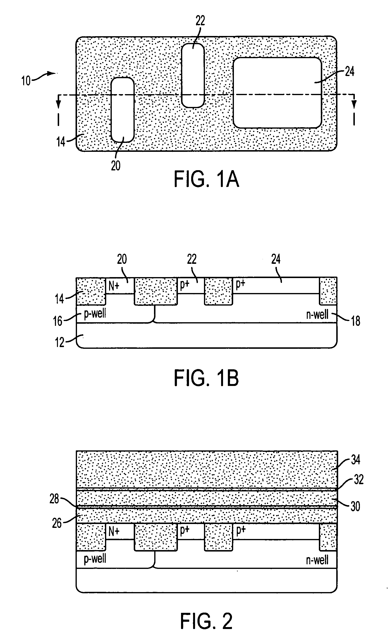
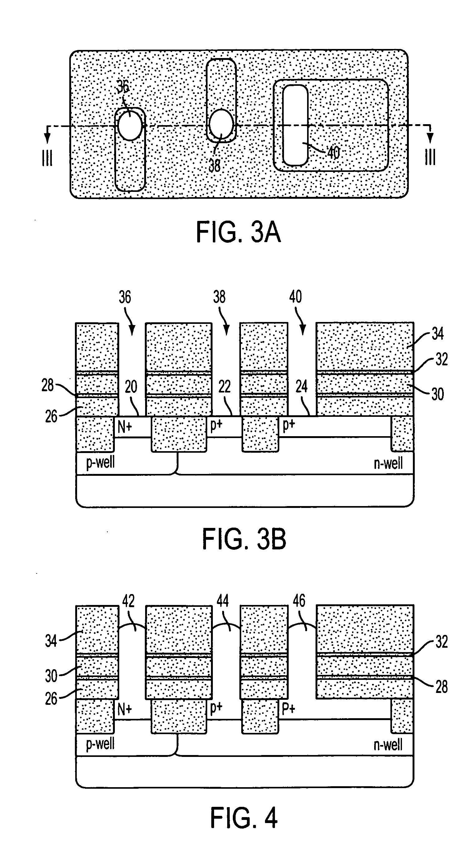
[0075] In the following detailed description, reference is made to an exemplary embodiment of the invention. The embodiment is described with sufficient detail to enable those skilled in the art to practice the invention, and it is to be understood that other embodiments may be employed, and that structural and electrical changes may be made without departing from the spirit or scope of the present invention.

[0076] The term “substrate” used in the following description may include any semiconductor-based structure that has an exposed semiconductor surface. Such structure must be understood to include silicon, silicon-on insulator (SOI), silicon-on sapphire (SOS), doped and undoped semiconductors, epitaxial layers of silicon supported by a base semiconductor foundation, silicon-germanium, germanium, gallium arsenide, and other semiconductor structures. Also, when reference is made to a substrate in the following description, previous process steps typical in the art and not specific...


PUM


Abstract

A vertical transistor having a wrap-around-gate and a method of fabricating such a transistor. The wrap-around-gate (WAG) vertical transistors are fabricated by a process in which source, drain and channel regions of the transistor are automatically defined and aligned by the fabrication process, without photolithographic patterning.

Description

FIELD OF THE INVENTION [0001] This invention relates to the field of semiconductor transistors, and more specifically to transistors which are suitable for use in high density semiconductor structures. BACKGROUND OF THE INVENTION [0002] There is ever-present pressure in the semiconductor industry to develop smaller and more highly integrated devices. As the demand increases for cheaper, faster, less power consuming yet more powerful integrated circuits such as microprocessors and memory devices, the transistor packing density of the integrated circuit must be similarly increased. [0003] As the industry standard approaches smaller and smaller scaled devices, problems with further advancement are presented and it becomes more difficult to produce sub-micron devices that can perform as desired. For example, in producing memory systems for such increasingly compact devices, the goal of expanding or, at least, maintaining memory capacity as cell size shrinks must be attained without reso...

Claims


Application Information

Patent Timeline
IPC IPC(8): H01L21/336H01L21/332
CPCH01L27/10814H01L27/10876H01L27/10885H01L29/78642H01L27/1203H01L29/42392H01L27/10891H01L29/66666H01L29/7827H10B12/315H10B12/053H10B12/488H10B12/482
Inventor TANG, SANH D.BURKE, ROBERT J.SRINIVASAN, ANAND
Owner MICRON TECH INC
Features
  • Generate Ideas
  • Intellectual Property
  • Life Sciences
  • Materials
  • Tech Scout
  • Unparalleled Data Quality
  • Higher Quality Content
  • 60% Fewer Hallucinations
Learn More