Semiconductor devices with graded dopant regions

a technology of dopant regions and semiconductor devices, applied in semiconductor devices, diodes, transistors, etc., can solve the problems of a small but finite role of majority carriers in modulating

Inactive Publication Date: 2006-03-09
GREENTHREAD
View PDF28 Cites 137 Cited by
  • Summary
  • Abstract
  • Description
  • Claims
  • Application Information

AI Technical Summary

Problems solved by technology

However, majority carriers also a small yet finite role in modulating the conductivity in BJTs.
It also brings new challenges because the required characteristics (electron transit and hole recom...

Method used


Image

  • Semiconductor devices with graded dopant regions
  • Semiconductor devices with graded dopant regions
  • Semiconductor devices with graded dopant regions

Examples


Embodiment Construction

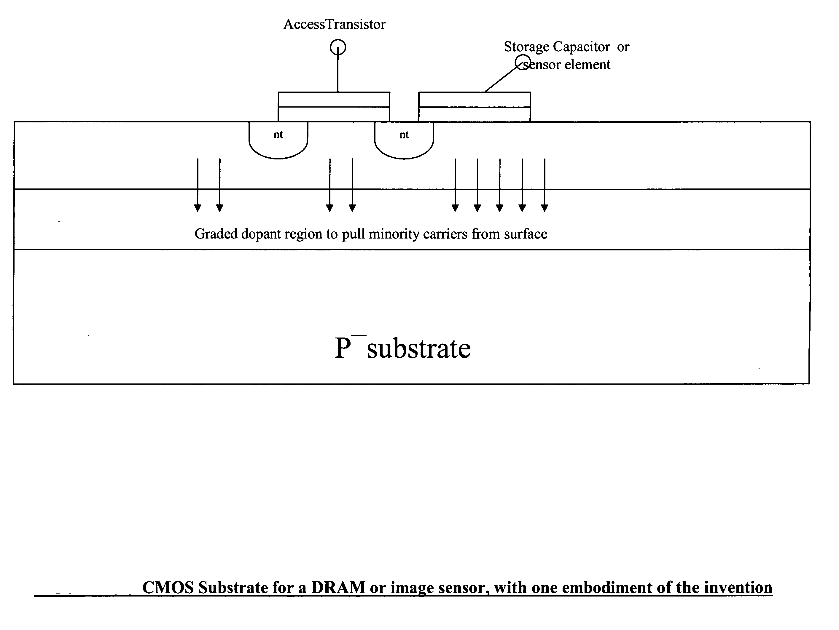
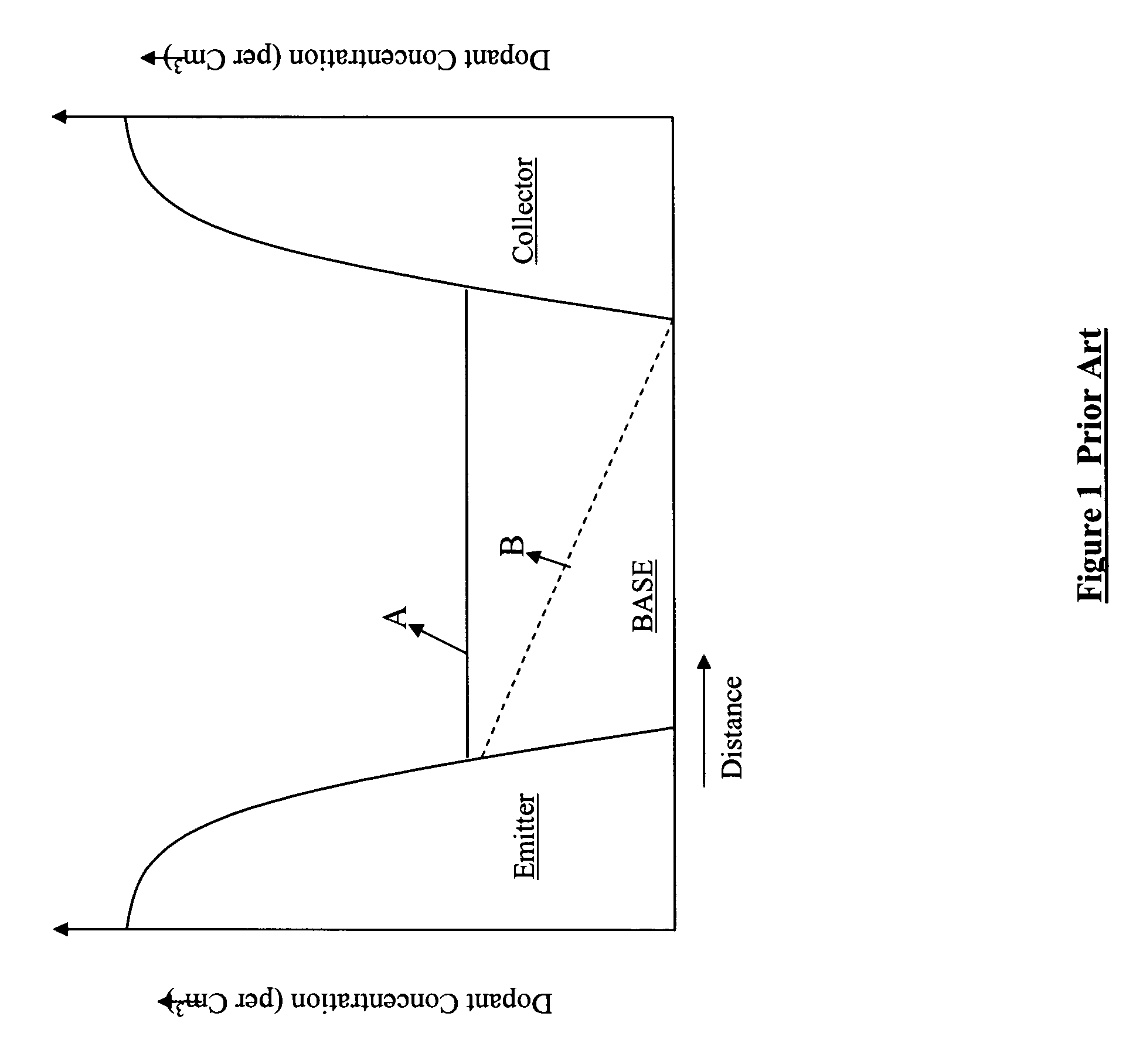
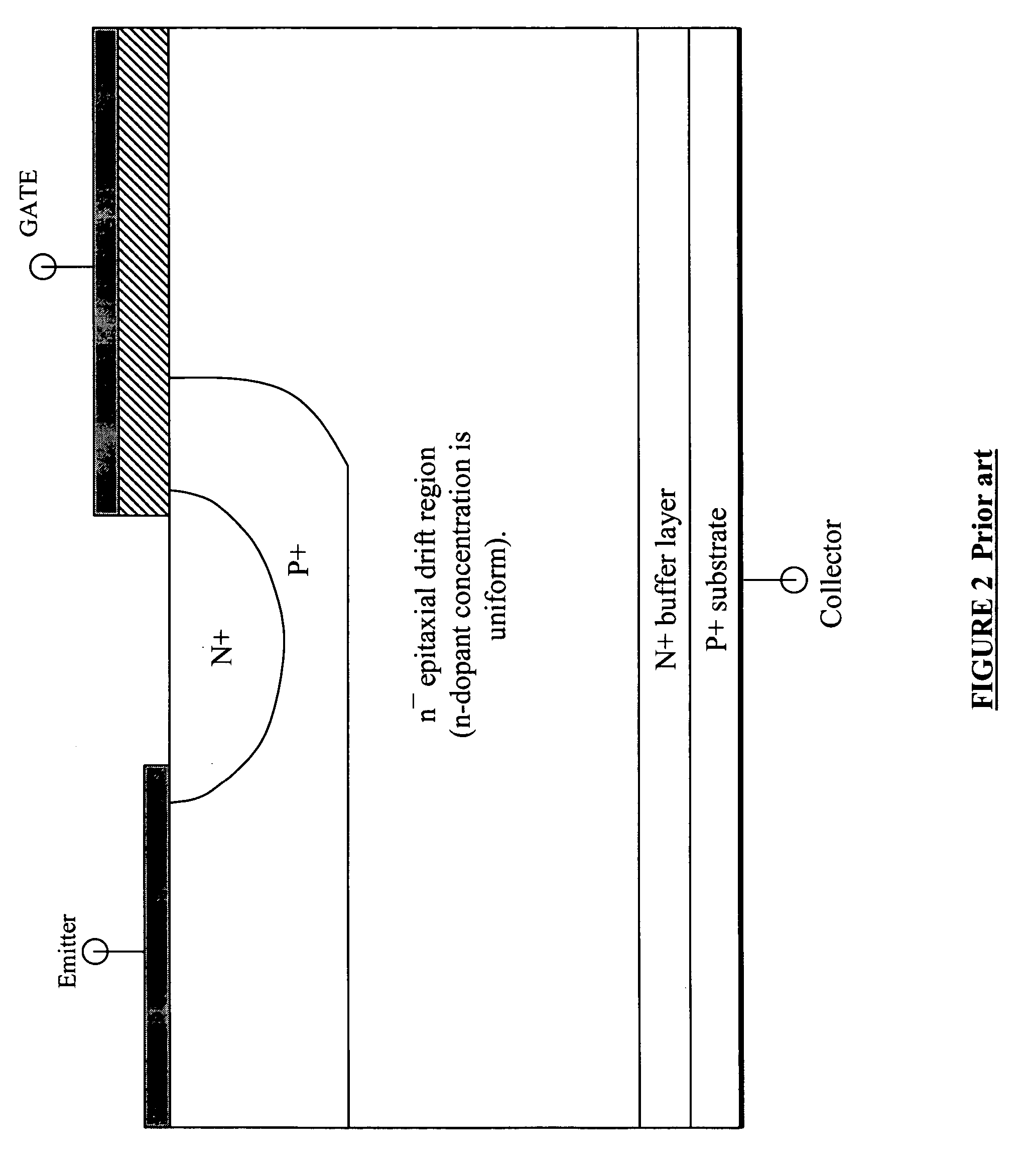
[0011] The relative doping concentrations of emitter and collector regions varies from 1018 to 1020 / cm3, where as the base region is 1014 to 1016 / cm3 depending on the desired characteristics of the BJT. In graded base p-n-p transistors, the donor dopant concentration may be 10 to 100× at the emitter-base junction, relative to the base-collector junction (1×). The gradient can be linear, quasi linear, exponential or complimentary error function. The relative slope of the donor concentration throughout the base, creates a suitable aiding drift electric field, to help the holes (p-n-p transistor) transverse from emitter to collector. Since the aiding drift field helps hole conduction, the current gain at a given frequency is enhanced, relative to a uniformly-doped-(base) BJT. The improvement in cut-off frequency (or, frequency at unity gain, fT) can be as large as 2×-5×. Similar performance improvements are also applicable to n-p-n transistors.

[0012] As illustrated in FIG. 4, in one e...


PUM


Abstract

Most semiconductor devices manufactured today, have uniform dopant concentration, either in the lateral or vertical device active (and isolation) regions. By grading the dopant concentration, the performance in various semiconductor devices can be significantly improved. Performance improvements can be obtained in application specific areas like increase in frequency of operation for digital logic, various power MOSFET and IGBT ICS, improvement in refresh time for DRAM's, decrease in programming time for nonvolatile memory, better visual quality including pixel resolution and color sensitivity for imaging ICs, better sensitivity for varactors in tunable filters, higher drive capabilities for JFET's, and a host of other applications.

Description

CROSS-REFERENCE TO RELATED APPLICATION [0001] This application is not related to any pending application. FIELD OF INVENTION [0002] This present invention relates to all semiconductor devices and systems. Particularly it applies to diffused diodes, avalanche diodes, Schottky devices, power MOS transistors, JFET's, RF bipolar transistors, IGBTs (Insulated Gate Bipolar Transistors), varactors, digital VLSI, mixed signal circuits and sensor devices including camera ICs employing CCD (Charge Coupled Device) as well as CMOS technologies. BACKGROUND OF INVENTION [0003] Bipolar Junction transistors (BJT) are minority carrier devices as the principle device conduction mechanism. However, majority carriers also a small yet finite role in modulating the conductivity in BJTs. Consequently, both carriers (electrons and holes) play a role in the switching performance of BJTs. The maximum frequency of operation in BJTs is limited by the base transit time as well as the quick recombination of the ...

Claims


Application Information

Patent Timeline
IPC IPC(8): H01L29/74
CPCH01L27/0214H01L27/10844H01L27/11521H01L29/36H01L27/14643H01L29/7395H01L27/11524H10B12/01H10B41/30H10B41/35H01L29/1095
Inventor RAO, G.R. MOHAN
Owner GREENTHREAD
Why Eureka
Try Eureka