
Method of self-assembling electronic circuitry and circuits formed thereby

Active Publication Date: 2006-03-09
IBM CORP
View PDF7 Cites 8 Cited by
  • Summary
  • Abstract
  • Description
  • Claims
  • Application Information

AI Technical Summary

Benefits of technology

[0008] An object of the invention is to minimize the number of lithographic steps. We demonstrate how this can be done in one lithographic step, thus saving money.
[0015] An exemplary method in accordance with the invention produces electronic circuits that self-assemble. The present invention avoids costly photolithography involving many steps and takes advantage of molecular transistor elements, fabricates nanowires for metallization, and capacitors, if needed, which are connected between circuit elements.

Problems solved by technology

However, the formation of these circuits requires multiple layer formation steps.
These processes are very expensive to perform and each layer adds cost to the manufacturing process of lithographically forming electronic circuits.
The smaller the size of the device, the more difficult it is to manufacture and, thus, the more expensive the device becomes to manufacture.
This trend is further complicated by the fact that, as the devices approach molecular scales, multistep lithographic approaches may not work at all due to lithographic constraints imposed by resolution and alignment.

Method used


Image

  • Method of self-assembling electronic circuitry and circuits formed thereby
  • Method of self-assembling electronic circuitry and circuits formed thereby
  • Method of self-assembling electronic circuitry and circuits formed thereby

Examples


first exemplary embodiment

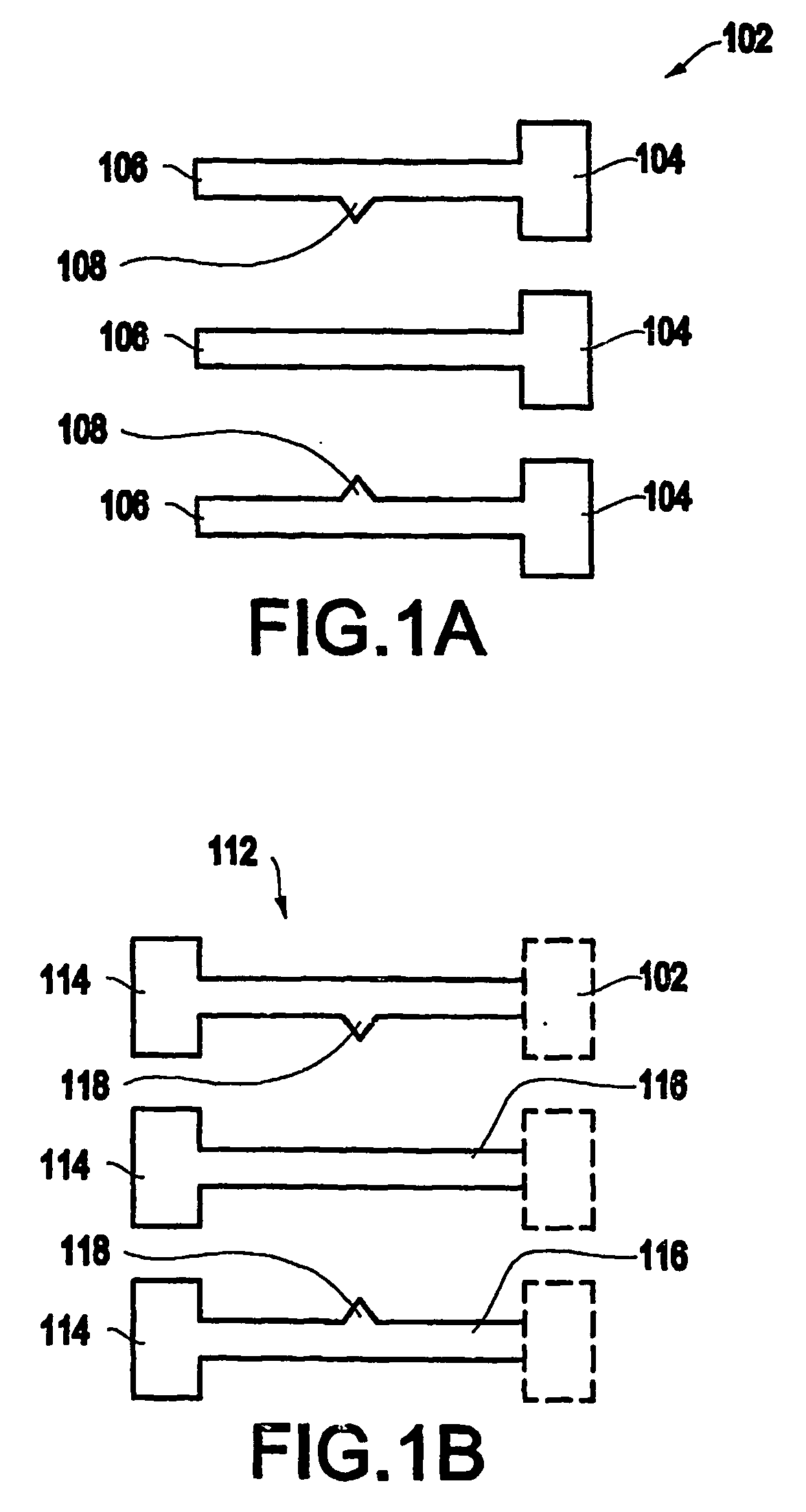
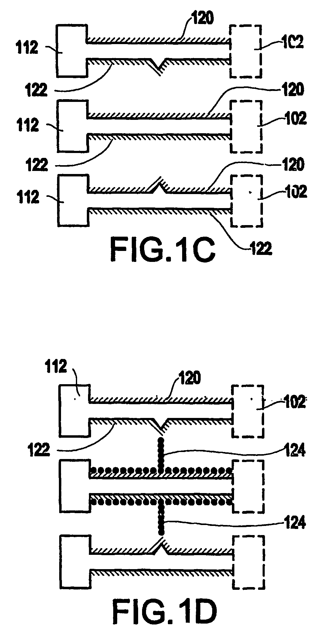
[0027] Referring to FIGS. 1A-1D, 2 and 4 in a first exemplary method in accordance with the invention, the method starts at step S400 and continues to step S402 where a substrate (not shown) such as oxidized silicon or an insulator is provided on a conducting plane which can be used as a ground plane.

[0028] In step S404, on this substrate, a one step shadow mask, or a lithographically defined area, is used to deposit a conducting layer which can be metallic or organic. A patterned gold layer 102 (FIG. 1A) illustrates an example of this layer. The gold layer 102 may be formed on an adhesion layer such as Ti (not shown). The gold layer 102 includes contacts 104, three elongated stripes 106 and pointed structures 108, which are also known as “field concentrators,” extending from the outer two stripes. The stripes are elongated here for illustrative purposes only. In an actual circuit, their shapes and dimensions will depend on the specific design of a system in which the inverter may ...

second exemplary embodiment

[0043]FIGS. 5A-5E illustrate a second exemplary method for forming a structure (e.g., a NAND gate 500 (completed structure shown schematically in FIG. 6)) in accordance with the invention.

[0044] In FIG. 5A, a metal (e.g., gold) layer 502 is formed on a substrate 501 (see FIG. 5C) by, for example, evaporation in a vacuum. The thickness of these films is in the tens of nm range. In these Figures, the metal (e.g., gold) lines L1-L7 are shown both as solid and broken lines. The solid lines are similar to those used in the inverter circuit and the broken lines will be used to provide for connections and crossovers, as described below. FIG. 5A also shows that lines L1, L3 and L5 include field concentrators 508 which will be used below.

[0045] As shown in FIGS. 5 and 6, one of the contacts pads 526 on line IA of the gold layer 502 will eventually form the output.

[0046] On top of this metal (e.g., gold) layer 502, an insulating layer 503 (only shown in FIG. 5C) is deposited followed by a ...

third exemplary embodiment

[0058] In yet a third exemplary method (not shown) of practicing the present invention, an electric field may be applied locally and without direct contact. In this exemplary method, a beam of electrons is focussed and applied to a line in a template containing a field concentrator. The beam of electrons may be generated by an electron beam machine and be focussed down to a nanometer in width. The beam of electrons will apply a charge to the line in the template and, therefore, will create a field around the line. If another line in the template is grounded, then a field gradient is established between the charged line and the grounded line. The field gradient is concentrated at the concentrator and the closest point on the grounded line. This field causes the nanoparticles to move and self assemble into a wire that will connect the two lines between the concentrator and the closest point on the grounded line.

[0059] The invention can also be easily tailored to produce other structu...


PUM


Abstract

A method of assembling a circuit includes providing a template, enabling a semiconductor material to self assemble on the template, and enabling self-assembly of a connection between the semiconductor material and the template to form the circuit and a circuit created by self-assembly.

Description

BACKGROUND OF THE INVENTION [0001] 1. Field of the Invention [0002] The present invention generally relates to a method of assembling electronic circuits and an electronic circuit formed using that method. More particularly, this invention relates to a method of enabling self-assembly of electronic circuitry and to self-assembled electronic circuits. [0003] 2. Description of the Related Art [0004] Formation of electronic circuits using lithographic techniques is well known. However, the formation of these circuits requires multiple layer formation steps. For example, one may have as many as 25 masking steps to form an electronic circuit using lithographic techniques. These processes are very expensive to perform and each layer adds cost to the manufacturing process of lithographically forming electronic circuits. [0005] It is also desirable to reduce the size of the electronic elements forming the circuit. The smaller the size of the device, the more difficult it is to manufacture a...

Claims


Application Information

Patent Timeline
IPC IPC(8): H01L31/117H01L21/98H01L23/12H01L51/00
CPCB82Y10/00H01L25/50H01L51/0595H05K1/0293H05K2203/105H01L2924/0002H05K2203/173H01L2924/00H10K10/701
Inventor CHAUDHARI, PRAVEEN
Owner IBM CORP
Learn More