Physical vapor deposition apparatus for depositing thin multilayer films and methods of depositing such films

a physical vapor deposition and multi-layer technology, applied in vacuum evaporation coatings, electrolysis components, coatings, etc., can solve the problems of increasing the cost and increasing the difficulty of conventional pvd tools to achieve the necessary performance in data storage and semiconductor applications. achieve the effect of high speed, uniformity and surface smoothness, and extreme control of thickness

Inactive Publication Date: 2006-03-16
VEECO INSTR
View PDF15 Cites 32 Cited by
  • Summary
  • Abstract
  • Description
  • Claims
  • Application Information

AI Technical Summary

Benefits of technology

[0014] The present invention creates a compact and economical PVD module that is capable of depositing thin film multi-layers with extreme control of thickness, uniformity and surface smoothness. The present invention creates a compact module capable of generating extremely well controlled multi-layer films by arranging multiple cathodes in a conical cluster about a single deposition zone while using two independently controlled (rotation and scanning) substrate motions to achieve the required film thickness, uniformity and surface smoothness parameters. The present invention does not require or utilize a shutter to control the film deposition.
[0015] The present invention relates to a compact multi-sputter source deposition chamber, with a confocal arrangement of the sputter sources and a deposition aperture to precisely define the deposition zone. ...

Problems solved by technology

Despite use of these uneconomical techniques, the resulting deposition uniformity is generally limited to 1% one standard deviation (i.e., sigma) of the deposited layer thickness.
However, rotating the substrate does not effect radial uniformity.
Therefore, the ability of conventional PVD tools to achieve the necessary performance in data storage and semiconductor applications is becoming more difficult and increasingly expensive.
Two primary weaknesses are intrinsic to the dial-index configuration.
One weakness is the need for a shutter to control the deposition and the effect of the shutter actuation time on the control of the thickness and uniformity of the film.
Another weakness in the design of dial-index PVD tools is the large size and consequent cost of the module or tool, which is driven by the cathode size of the sputter source required to provid...

Method used


Image

  • Physical vapor deposition apparatus for depositing thin multilayer films and methods of depositing such films
  • Physical vapor deposition apparatus for depositing thin multilayer films and methods of depositing such films
  • Physical vapor deposition apparatus for depositing thin multilayer films and methods of depositing such films

Examples


Embodiment Construction

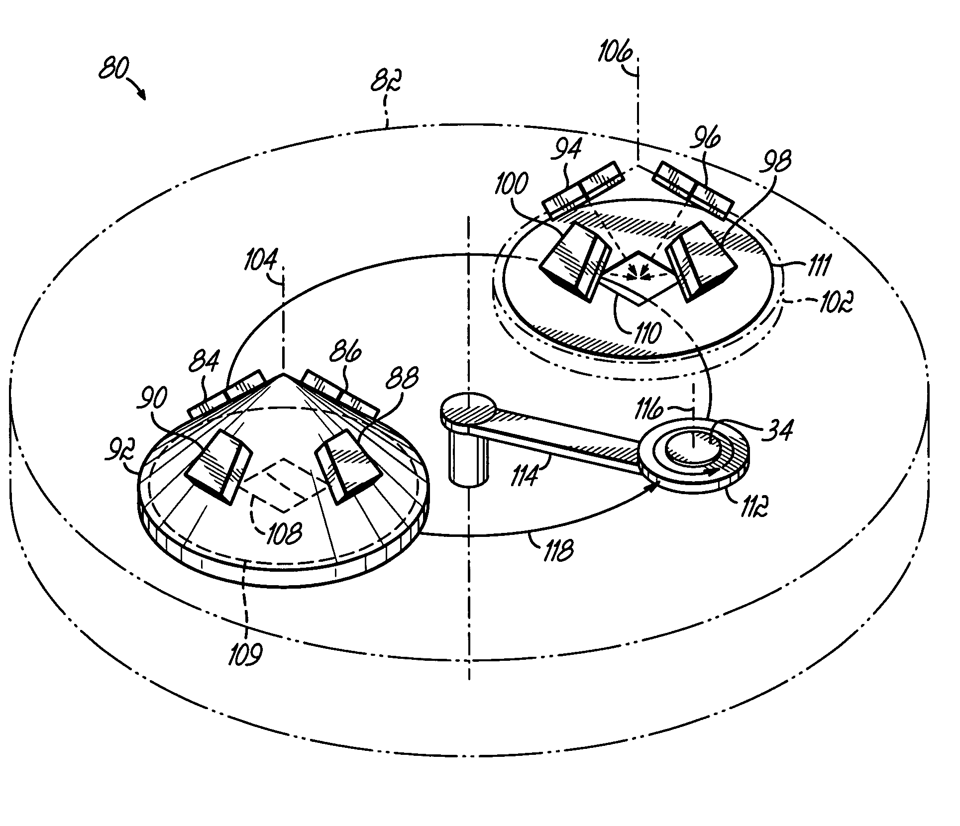
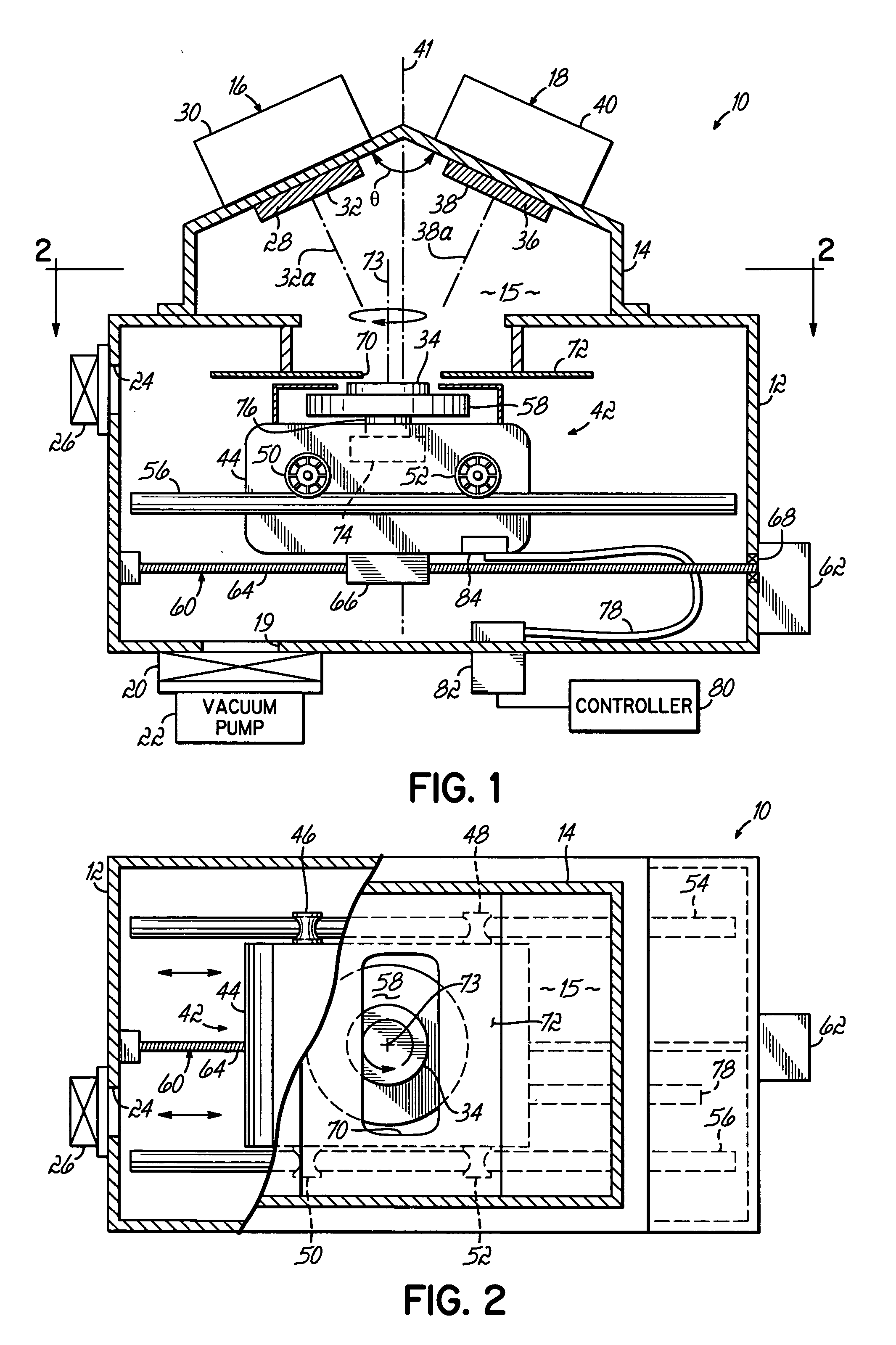
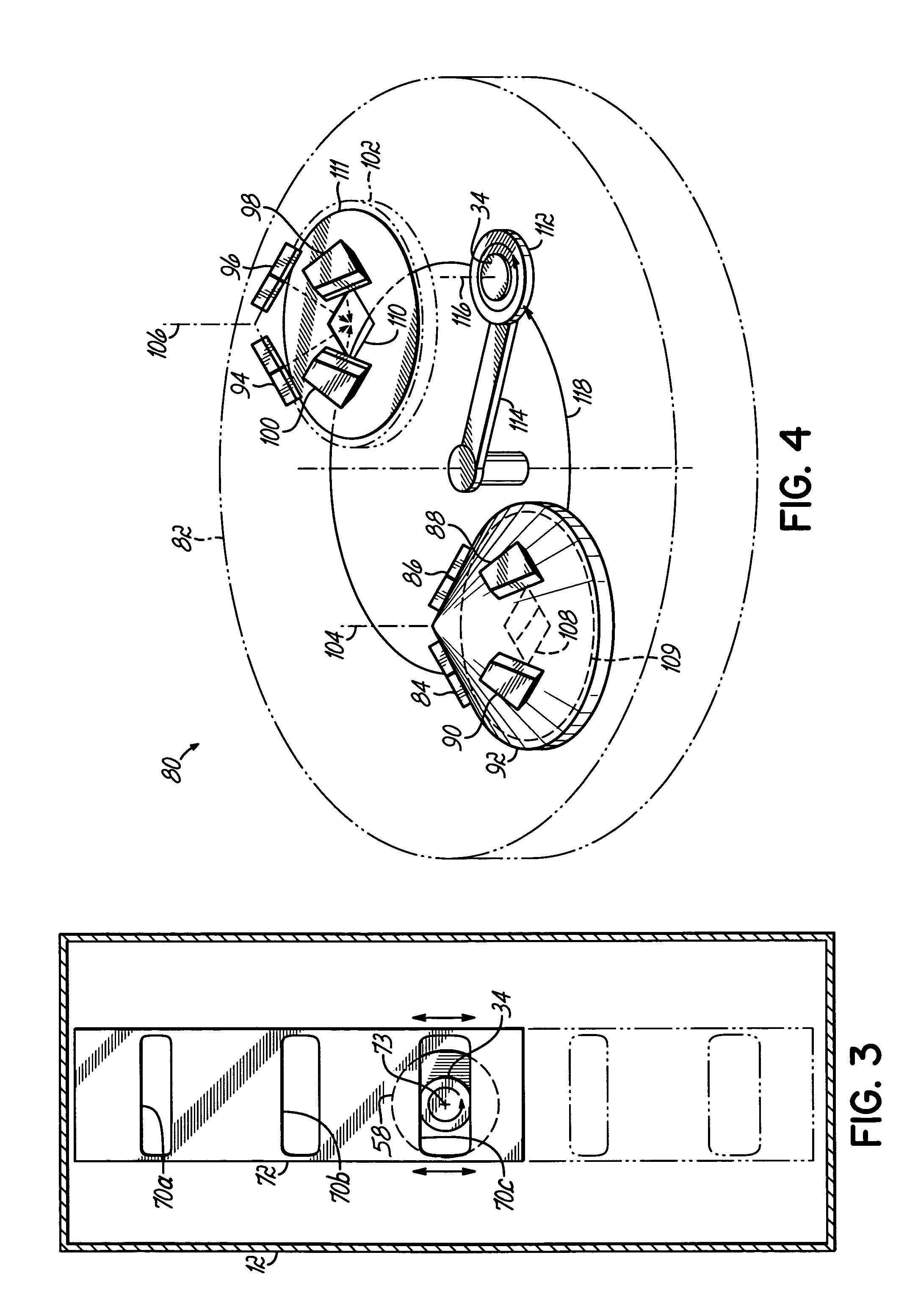
[0023] With reference to FIG. 1, a processing apparatus 10 in accordance with the invention includes a vacuum chamber 12 and a chamber lid 14 defining an evacuable or controlled atmosphere volume 15. A set or cluster of deposition sources 16, 18 is mounted on the chamber lid 14. Typically, the apparatus 10 will include between two and six individual deposition sources, although only two deposition sources 16, 18 are shown in FIG. 1. An exhaust port 19 of the vacuum chamber 12, which is isolated from the surrounding environment, is, selectively coupled by a gate valve 20 with a vacuum pump 22 for evacuating the controlled atmosphere volume 15. The vacuum chamber 12 is also supplied with process gases as understood by persons of ordinary skill in the art. The controlled atmosphere volume 15 of vacuum chamber 12 is accessed through a substrate load port 24. The load port 24 is normally isolated from the vacuum chamber 12 by a suitable isolation valve 26. The isolation valve 26 may be a...


PUM

PropertyMeasurementUnit
Thicknessaaaaaaaaaa
Speedaaaaaaaaaa
Shapeaaaaaaaaaa

Abstract

A compact and economical physical vapor deposition (PVD) module for depositing thin film multi-layers with extreme control of thickness, uniformity and surface smoothness. The module includes multiple deposition sources positioned in a conical cluster with confocal arrangement about a single common deposition zone that is defined by a deposition aperture and a substrate carrier with two independently controlled (rotation and scanning) substrate motions. A substrate carrier rotates the substrate at high speed and translates the substrate through the deposition zone. The module lacks a shutter for controlling the film deposition process. Methods of depositing thin film multi-layers are also described.

Description

FIELD OF THE INVENTION [0001] The present invention relates to apparatus and methods for processing substrates like semiconductor wafers and data storage components and, more particularly, to improved apparatus and methods for depositing one or more layers or thin films of material on such substrates. BACKGROUND OF THE INVENTION [0002] Most physical vapor deposition (PVD) modules and tools currently in use by the data storage, semiconductor and related industries deposit materials with the substrate stationary and depend on the use of oversize targets, in relation to the substrate size, or extremely long target-to-substrate distances, to achieve uniformity. Despite use of these uneconomical techniques, the resulting deposition uniformity is generally limited to 1% one standard deviation (i.e., sigma) of the deposited layer thickness. Feature size reductions in the data storage and semiconductor industries have resulted in requirements for thin films with sub-nanometer control of thi...

Claims


Application Information

Patent Timeline
IPC IPC(8): C23C14/00C23C14/32
CPCC23C14/352H01J37/3447C23C14/505
Inventor REISS, IRA
Owner VEECO INSTR
Why Eureka
Try Eureka