Method and system for inspecting specimen

Inactive Publication Date: 2006-03-16
JEOL LTD
View PDF23 Cites 18 Cited by
  • Summary
  • Abstract
  • Description
  • Claims
  • Application Information

AI Technical Summary

Benefits of technology

[0023] According to the third specimen inspection system based on the present invention, a voltage produced during scanning of the beam is detected via one probe. An electrical current produced during scanning of the beam is detected via the other pr

Problems solved by technology

In the prior art potential difference imaging method, the difference in secondary electron emission efficiency between positively and n

Method used


Image

  • Method and system for inspecting specimen
  • Method and system for inspecting specimen
  • Method and system for inspecting specimen

Examples


Example

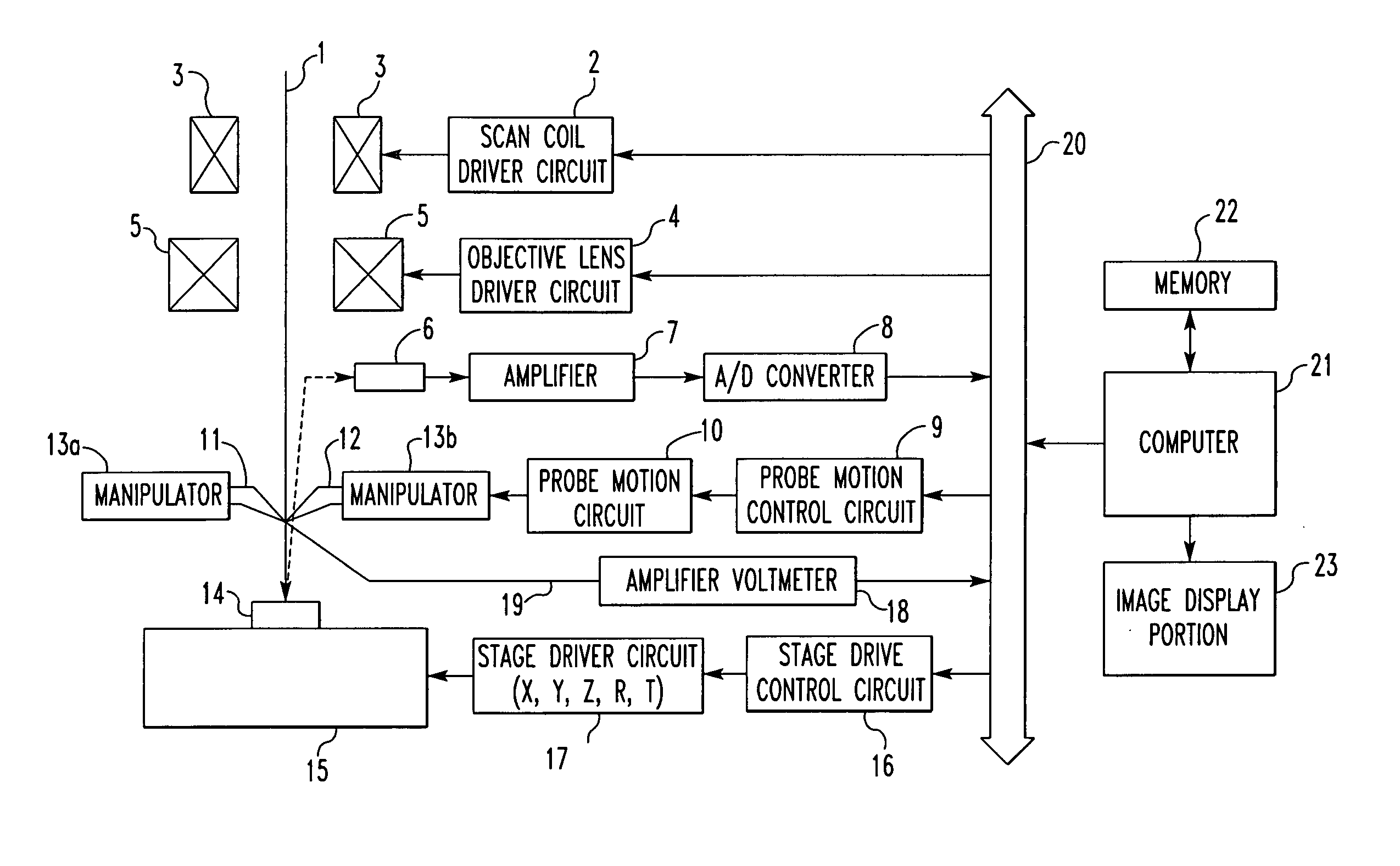
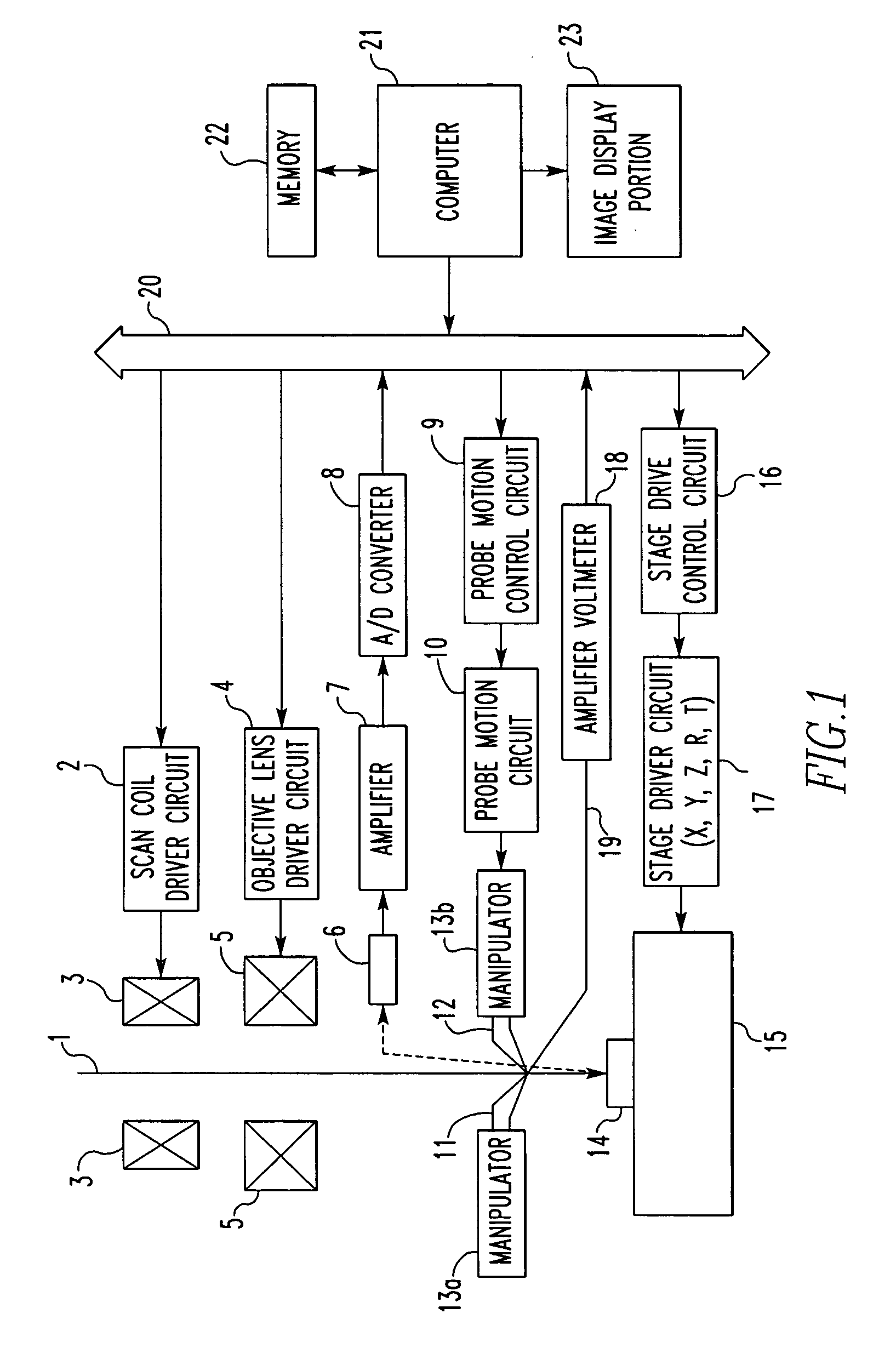
[0038]FIG. 1 is a block diagram illustrating a first embodiment of the present invention. Indicated by numeral 1 is an incident beam of electrons or ions. Scan coils 3 are driven by a scan coil driver circuit 2. An objective lens 5 is driven by an objective lens driver circuit 4.

[0039] A signal such as a secondary electron signal produced from a specimen is detected by a detector 6. The output from the detector 6 is amplified by an amplifier 7. The output from the amplifier 7 is converted into digital image data by an A / D converter 8. A probe motion control circuit 9 produces a control signal for moving probes (described in detail later). The output from the probe motion control circuit 9 is received by a probe motion circuit 10. The position of a first probe 11 is moved by the probe motion circuit 10. Indicated by numeral 12 is a second probe. Manipulators 13a and 13b drive the probes 11 and 12, respectively. For example, piezoelectric devices are used as the manipulators 13a and ...

Example

[0057]FIG. 5 shows a second embodiment of the present invention. Like components are indicated by like reference numerals in both FIGS. 1 and 5. Only those portions of FIG. 5 which are different from FIG. 1 are described. In FIG. 5, an insulating portion 30 is placed on the specimen stage 15. The specimen 14 is placed on the insulating portion 30. A deposition unit 31 marks given positions on the specimen 14 under control of a control circuit 32. The voltage signal from the second probe 12 is received by a voltage amplifier 33. The absorption current from the first probe 11 is received by a current amplifier 34. The outputs of the voltage amplifier 33 and current amplifier 34 are connected with the bus 20. The output signals from the amplifiers 33 and 34 are converted into digital image data by an A / D converter (not shown) and then supplied to the bus 20.

[0058]FIG. 6 shows an example of the specimen stage 15. The insulating portion 30 is formed on the stage 15. The specimen 14 is p...

Example

[0072]FIG. 8 shows a third embodiment of the present invention. Like components are indicated by like reference numerals in both FIGS. 5 and 8. This embodiment is characterized in that an ion beam irradiation apparatus is mounted in addition to the electron beam irradiation apparatus. The ion beam irradiation apparatus has a beam deflector 41 for deflecting an incident ion beam 40. The apparatus further includes an objective lens 42 for directing the ion beam at a specimen 14. The deflector 41 is controlled by a deflector driver circuit 43. This embodiment is identical with the embodiment of FIG. 5 in other respects. The microscope column for ion beam is so positioned that the same portion as the field of view observed with an electron beam can be observed. The operation of the system constructed in this way is described below.

[0073] A potential distribution image of the specimen 14 is obtained using the electron beam irradiation apparatus by manipulations performed in the same way...


PUM


Abstract

Method and system for obtaining a potential distribution image of a specimen using two probes having two probes contacted with a patterned surface of the specimen, a scanning unit for scanning a beam of electrons or ions over the specimen, a potential detection unit for detecting the electric potential at an arbitrary position on the specimen using the probes, and an acquisition unit for obtaining a potential distribution image of the specimen while synchronizing the output from the potential detection unit with the scanning of the beam.

Description

BACKGROUND OF THE INVENTION [0001] 1. Field of the Invention [0002] The present invention relates to a method and system for inspecting a specimen using at least one probe. [0003] 2. Description of Related Art [0004] Known specimen inspection systems for measuring the physical properties of a specimen in a scanning electron microscope (SEM) include an inspection system using an electron beam-induced current (EBIC) method and an inspection system using an electron beam LSI tester or cathodoluminescence. Of these systems, inspection systems using cathodoluminescence measure physical properties of specimens by a technique utilizing optical physical properties. On the other hand, in inspection systems using EBIC, a lead wire or interconnect line connected with a probe in contact with a wide-area electrode (usually known as a pad) or an interconnect line bonded to the pad is brought to the outside of the SEM specimen chamber, and the EBIC is measured outside the SEM. [0005] One conventio...

Claims


Application Information

Patent Timeline
IPC IPC(8): G01N23/00G21K7/00
CPCG01N23/225H01J37/244H01J2237/24592H01J2237/24495H01J2237/24564H01J37/28
Inventor NOKUO, TAKESHIKAWASE, SATORUMOURI, TADAHARU
Owner JEOL LTD
Why Eureka
Try Eureka