Method of manufacturing semiconductor device, semiconductor device, and mounting structure of semiconductor device

a technology of mounting structure and semiconductor device, which is applied in the direction of semiconductor device, semiconductor/solid-state device details, electrical apparatus, etc., can solve the problems of lowering mounting reliability, reducing mounting cost, and resin (the adhesive) being unable to be prevented from remaining between the land and the bump, so as to achieve high-density mounting and reduce mounting cost. , the effect of enhancing mounting reliability

Inactive Publication Date: 2006-03-16
SEIKO EPSON CORP
View PDF6 Cites 7 Cited by
  • Summary
  • Abstract
  • Description
  • Claims
  • Application Information

AI Technical Summary

Benefits of technology

[0043] According to the mounting structure of the semiconductor device, since the mounting structure is formed by one of the methods of manufacturing the semiconductor device, the mounting cost can be reduced by eliminating any dedicated devices as described above. And further, since the resin can be avoided from

Problems solved by technology

Therefore, the dedicated devices required therefor problematically raise the mounting cost.
Further, in the method in which the resin is provided to the substrate side and the semiconductor chip is bonded thereon by a face-down bonding process, since a bump of the semiconductor chip is connected to a land (a conductive section) on the substrate while pushing through the resin to move aside, the resin (the adhesive) cannot be prevented from remaining between the land and the bump.
And, the land and the bump could be exfoliated from each other because of the difference in the thermal expansion coef

Method used


Image

  • Method of manufacturing semiconductor device, semiconductor device, and mounting structure of semiconductor device
  • Method of manufacturing semiconductor device, semiconductor device, and mounting structure of semiconductor device
  • Method of manufacturing semiconductor device, semiconductor device, and mounting structure of semiconductor device

Examples


Embodiment Construction

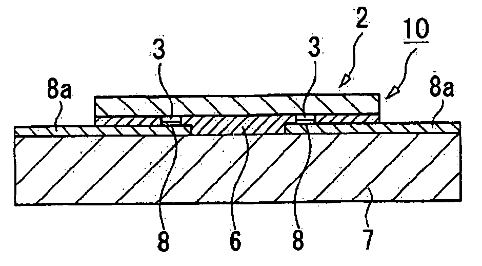
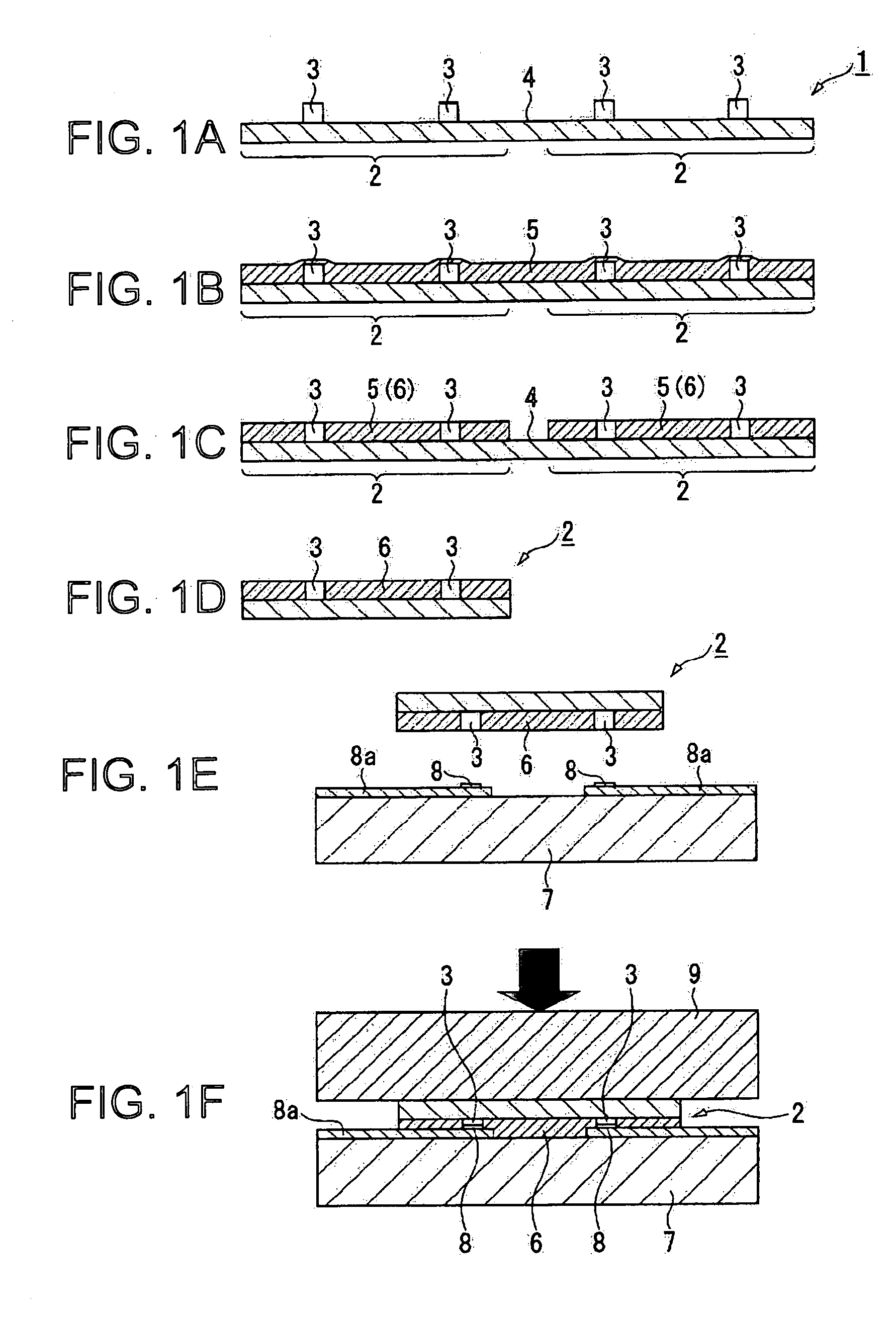
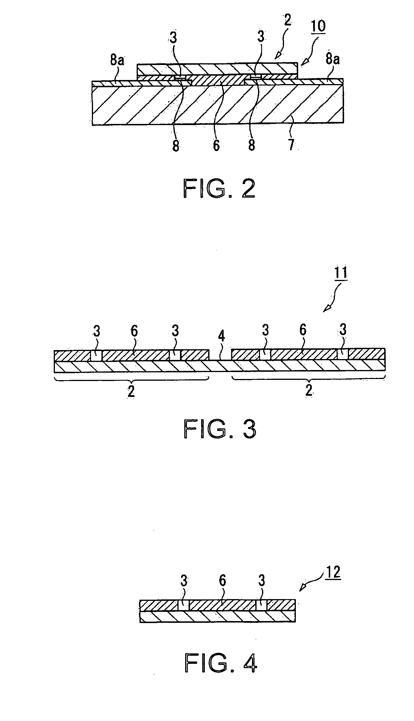
[0050] The invention will be explained hereinafter in detail. FIGS. 1A through 1F are schematic views for explaining processes of a mounting method of a semiconductor, which is an embodiment of the invention.

[0051] In the present embodiment, firstly a wafer 1 made of silicon is prepared as shown in FIG. 1A. In the wafer 1, there are a number of semiconductor chips 2 each equipped with various components formed thereon and further equipped with a number of bumps 3 formed on the side of the active surface. The bump 3 is formed of, for example, gold with an electrolytic plating process, or of a laminated structure of nickel and gold with an electroless plating process, and shaped like a cylinder or a prism having a height in a range of, for example, about 5 through 30 μm. Alternatively to the above, other known bumps such as a wire bump made by processing a gold wire to form a ball-shaped member, or a solder bump formed from solder can also be adopted.

[0052] In this case, the wafer 1...


PUM


Abstract

A method of manufacturing a semiconductor device, including the following steps, forming a resin layer on a surface of a semiconductor chip, the surface is provided with a bump formed thereon, the resin layer having photosensitivity and adhesiveness, exposing an upper surface of the bump by removing a part of the resin layer right above the bump by exposing and then developing the resin layer, and bonding the semiconductor chip provided with a resin film formed of the resin layer face-down to a substrate, the bump of the semiconductor chip and a conductive section of the substrate being electrically connected by the resin film functioning as an adhesive.

Description

RELATED APPLICATIONS [0001] This application claims priority to Japanese Patent Application Nos. 2004-268116 filed Sep. 15, 2004; 2005-088713 filed Mar. 25, 2005; and 2005-210067 filed Jul. 20, 2005 which are hereby expressly incorporated by reference herein in their entirety. BACKGROUND OF THE INVENTION [0002] 1. Technical Field [0003] The present invention relates to a semiconductor device equipped with a semiconductor chip, a method of manufacturing the semiconductor device by a face-down bonding process, and a mounting structure of the semiconductor device. [0004] 2. Related Art [0005] As a mounting method of a semiconductor chip by a face-down bonding process, a method using an anisotropic conductive membrane (See, for example, Japanese Unexamined Patent Publication No. 4-32171.) composed of anisotropic conductive paste (ACP) or an anisotropic conductive film (ACF) and a method using insulation resin for bonding (See, for example, Japanese Unexamined Patent Publication No. 4-82...

Claims


Application Information

Patent Timeline
IPC IPC(8): H01L21/44H01L23/48
CPCH01L23/544H01L24/81H01L2224/73204H01L2224/32225H01L2224/16225H01L2223/54453H01L2224/13144H01L2224/16H01L2224/274H01L2224/81801H01L2224/83191H01L2924/01013H01L2924/01029H01L2924/01033H01L2924/01049H01L2924/01078H01L2924/01079H01L2924/01082H01L2924/09701H01L2924/01005H01L2924/01006H01L2924/0105H01L2924/01075H01L2924/014H01L2924/00H01L2224/73104H01L2224/81191H01L2924/00011H01L2924/00014H01L2924/15787H01L2924/15788H01L2224/0401H01L21/52
Inventor HASHIMOTO, NOBUAKI
Owner SEIKO EPSON CORP
Why Eureka
Try Eureka