Check patentability & draft patents in minutes with Patsnap Eureka AI!

Measurement method of electron beam current, electron beam writing system and electron beam detector

a measurement method and beam current technology, applied in the field of measurement methods of electron beam current, an electron beam writing system and an electron beam detector, can solve the problems of long detection signal lines from the electron beam detecting device to the latter-stage measurement circuit, difficult to accurately measure such a weak and high-speed beam current from the viewpoint of signal/noise ratio, etc., to achieve high dimensional accuracy

Active Publication Date: 2006-03-23
HITACHI HIGH-TECH CORP +1
View PDF10 Cites 47 Cited by
  • Summary
  • Abstract
  • Description
  • Claims
  • Application Information

AI Technical Summary

Benefits of technology

[0016] Therefore, an object of the present invention is to provide a measurement method of electron beam current, an electron beam writing system and an electron beam detector which are required to form a pattern on a sample with high dimensional accuracy.
[0023] In this manner, the accurate measurement in which the influence of noise overlapped in the long detected signal line inherent in the electron beam wiring system is reduced as much as possible can be realized. Also, it becomes possible to simultaneously measure a plurality of electron beams with high accuracy.
[0025] It becomes possible to perform the accurate measurement of electron beam current in which the noise overlapped in a detected signal line is reduced as much as possible, and the dose of irradiation in the electron beam writing system can be controlled with high accuracy.

Problems solved by technology

Since the beam current becomes weak in the writing of the microscopic patterns, the accurate current measurement is difficult in the conventional beam current measurement using the Faraday cup.
Therefore, the accurate measurement of such a weak and high-speed beam current by the usual Faraday cup and an ammeter is difficult from the viewpoint of the signal / noise ratio.
Therefore, the detected signal line from the electron beam detecting device to the latter-stage measurement circuit becomes long.
In the case where the weak and high-speed signals are detected like in the electron beam writing system using multiple beams, if the conventional method using the Faraday cup or the method in which the signals are integrated in the latter-stage integrating circuit is used, the error occurs in the measurement of the current due to the noise overlapped on the long transmission path from the electron beam detecting device to the latter-stage measurement circuit (integrating circuit or amplifier circuit), and the improvement of the measurement accuracy is hindered.

Method used


Image

  • Measurement method of electron beam current, electron beam writing system and electron beam detector
  • Measurement method of electron beam current, electron beam writing system and electron beam detector
  • Measurement method of electron beam current, electron beam writing system and electron beam detector

Examples


first embodiment

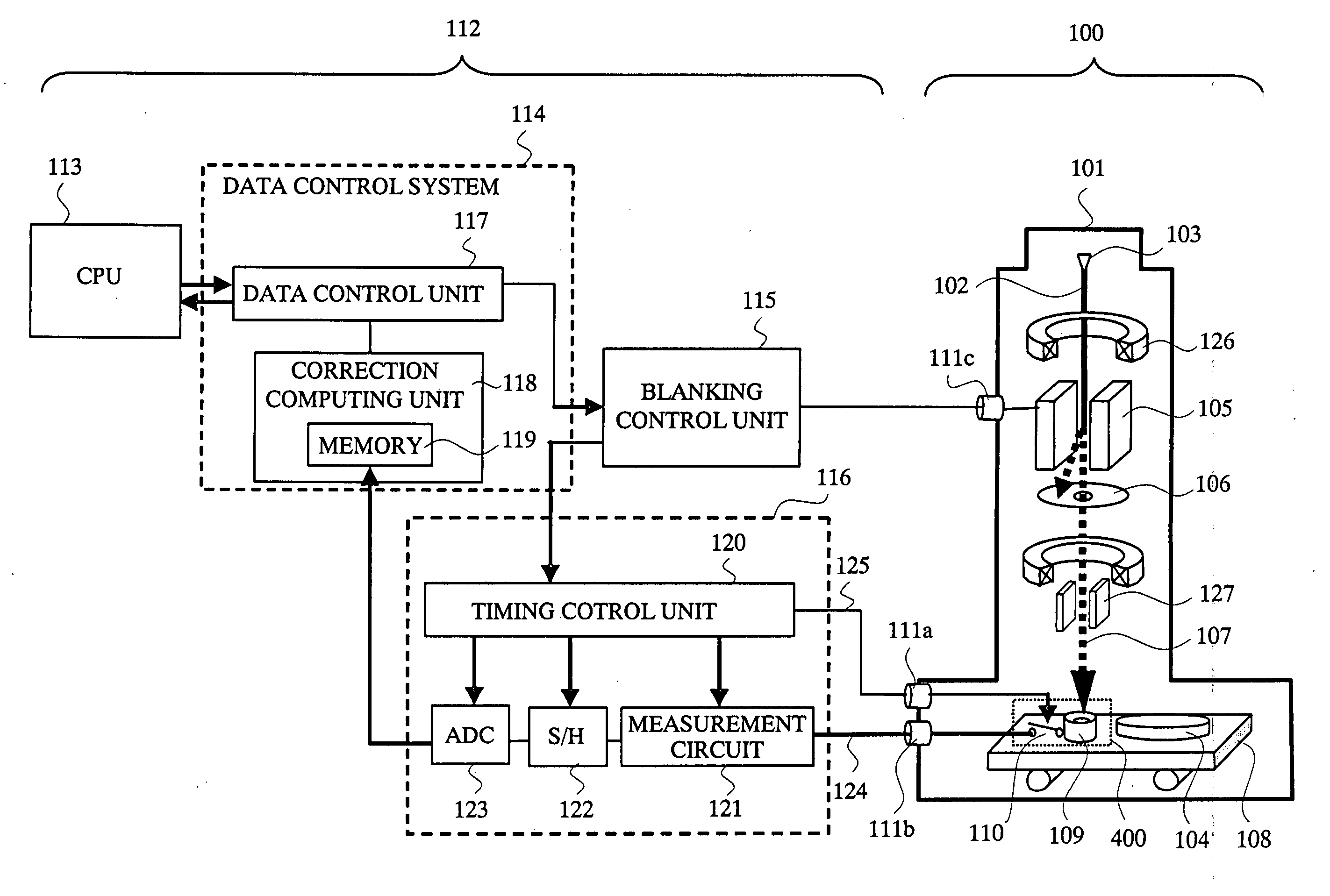
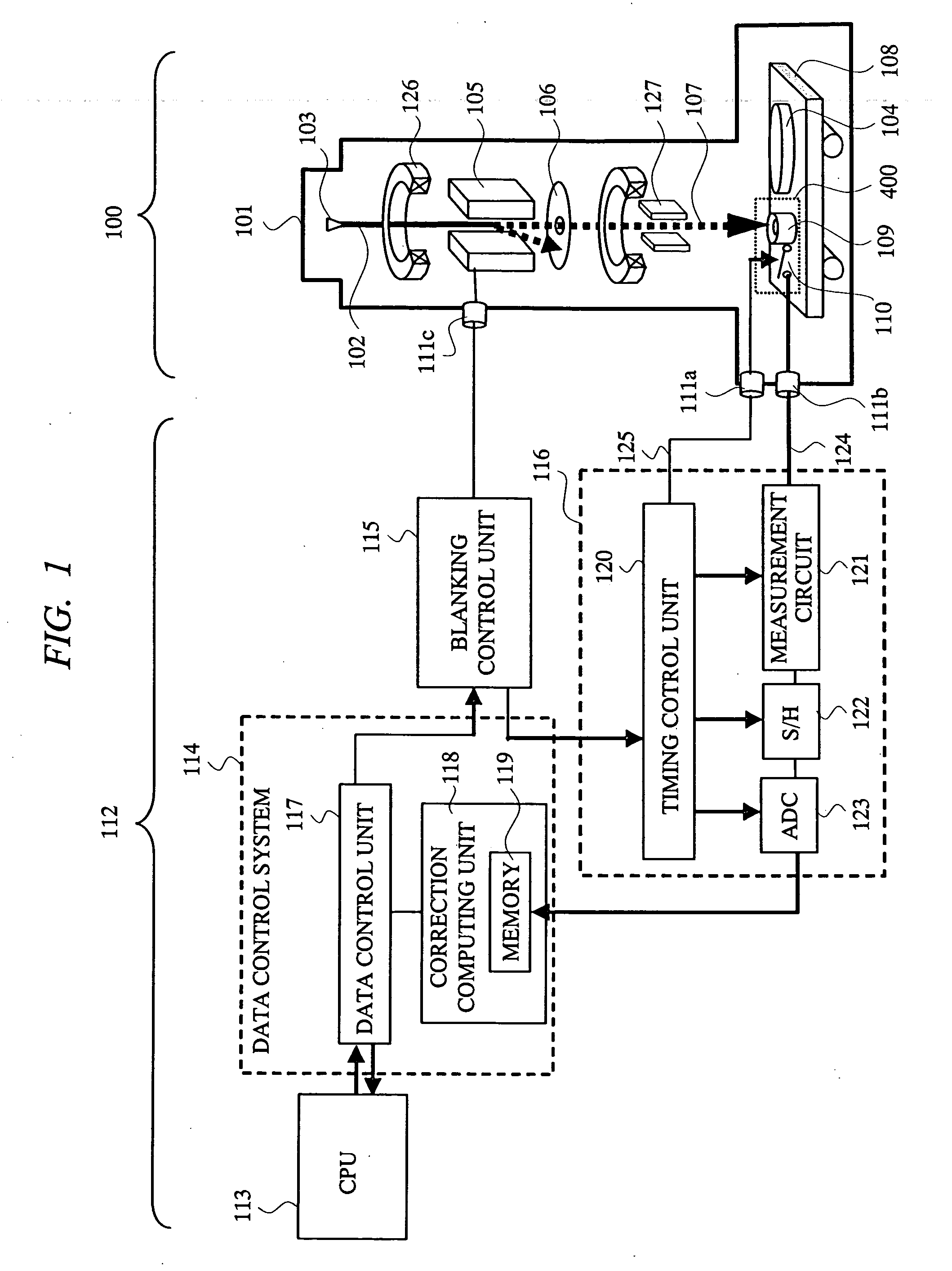
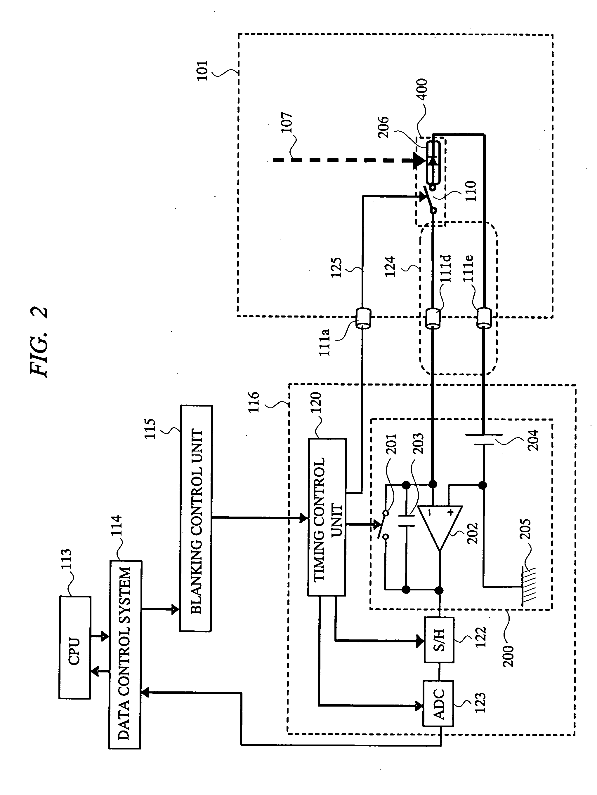
[0034]FIG. 1 is a block diagram showing a principal part of the electron beam writing system according to the first embodiment of the present invention, FIG. 2 is a block diagram showing an example of the case where an integrating circuit is used as a measurement circuit and a semiconductor diode is used as an electron beam detecting device in the electron beam writing system according to the first embodiment, FIG. 3 is a diagram showing, the timings in the beam current measurement, FIG. 4A and FIG. 4B are block diagrams showing the electron beam detector in which an electron beam detecting device, a charging element and a switch are incorporated, and FIG. 5 is a diagram showing the arrangement of cable terminals (hermetic connector).

[0035] First, an example of the configuration of the electron beam writing system according to the first embodiment will be described with reference to FIG. 1. The electron beam writing system according to the first embodiment is, for example, a writin...

second embodiment

[0080]FIG. 6 is a block diagram showing the principal part of the electron beam writing system using multiple beams according to the second embodiment of the present invention, and FIG. 7 is a diagram showing the configuration of the electron beam detector in the electron beam writing system using multiple beams according to the second embodiment.

[0081] First, an example of the configuration of the electron beam writing system using multiple beams according to the second embodiment-will be described with reference to FIG. 6. The electron beam writing system using multiple beams according to the second embodiment is, for example, a writing system using a plurality of electron beams and is comprised of an evacuated vacuum column 500, an electron gun 501 for generating electron beam 502, collimator lens 503, an aperture array 504, a lens array 505, a blanking electrode array 507 and a blanking aperture 508 for turning on / off the electron beams 506, first projection lens 509, a main de...

third embodiment

[0096] In this embodiment, further system, apparatus and components are disclosed.

[0097] An electron beam detector comprises an electron beam detecting element, a charging element for accumulating current detected by said electron beam detecting element as electric charge, and a switch for opening / closing output of said charging element, wherein said electron beam detecting element, said charging element and said switch are formed in the same semiconductor substrate.

[0098] An electron beam writing system comprises multiple beam generating means for generating a plurality of electron beams, an electron beam detecting device array comprised of a plurality of electron beam detecting devices which simultaneously detect electron beam current of said plurality of electron beams, a plurality of transmitting means for transmitting detected signals from said plurality of electron beam detecting devices, a plurality of measurement means for measuring said detected signals, blanking means fo...


PUM

PropertyMeasurementUnit
diameteraaaaaaaaaa
forward voltageaaaaaaaaaa
device capacitanceaaaaaaaaaa

Abstract

A technology capable of reducing the influence of the noise overlapped in a long transmission line when accurately measuring weak beam current in an electron beam writing system and capable of accurately and efficiently measuring weak beam current in a beam writing system using multiple beams is provided. With using a switch for connecting and disconnecting an electron beam detecting device and a detected signal line, the electron beam detecting device is disconnected from the detected signal line to accumulate the detected signals in the electron beam detecting device during the beam current measurement. Simultaneously with the finish of the measurement, the electron beam detecting device and the detected signal line are connected to measure the accumulated signals. Also, in order to simultaneously perform the measurement method, a plurality of electron beam detecting devices and switches are used to simultaneously measure a plurality of electron beams with high accuracy.

Description

CROSS-REFERENCE TO RELATED APPLICATION [0001] The present application claims priority from Japanese Patent Application No. JP 2004-261776 filed on Sep. 9, 2004, the content of which is hereby incorporated by reference into this application. TECHNICAL FIELD OF THE INVENTION [0002] The present invention relates to a measurement method of electron beam current, an electron beam writing system and an electron beam detector. More particularly, the present invention relates to a technology effectively applied to the method and means for measuring the average current amount of electron beam and pulse beam and to the electron beam writing system which uses multiple electron beams and pulse beams to perform the writing. BACKGROUND OF THE INVENTION [0003] In the technology examined by the inventors of the present invention, for example, in the electron beam writing system used in the manufacture of a semiconductor integrated circuit device (LSI), the LSI has been increasingly miniaturized, th...

Claims


Application Information

Patent Timeline
Patent Type & Authority Applications(United States)
IPC IPC(8): G01N23/00
CPCB82Y10/00B82Y40/00H01J2237/30472H01J37/243H01J37/3177G01R19/0061
Inventor SAKAKIBARA, MAKOTONAKAYAMA, YOSHINORIOHTA, HIROYASOHDA, YASUNARITANAKA, NORIYUKISOMEDA, YASUHIRO
Owner HITACHI HIGH-TECH CORP
Features
  • R&D
  • Intellectual Property
  • Life Sciences
  • Materials
  • Tech Scout
  • Unparalleled Data Quality
  • Higher Quality Content
  • 60% Fewer Hallucinations
Learn More