

Polysilicon sidewall spacer lateral bipolar transistor on SOI
a polysilicon sidewall spacer and bipolar transistor technology, applied in the direction of semiconductor devices, basic electric elements, electrical equipment, etc., can solve the problems of increasing the cost of wafers by approximately 1.3 times, and the cost of implementing a 0.13 m sige bicmos more than five times the cost of the 0.35 m process
- Summary
- Abstract
- Description
- Claims
- Application Information
AI Technical Summary
Benefits of technology
Problems solved by technology
Method used
Image

Examples
Embodiment Construction
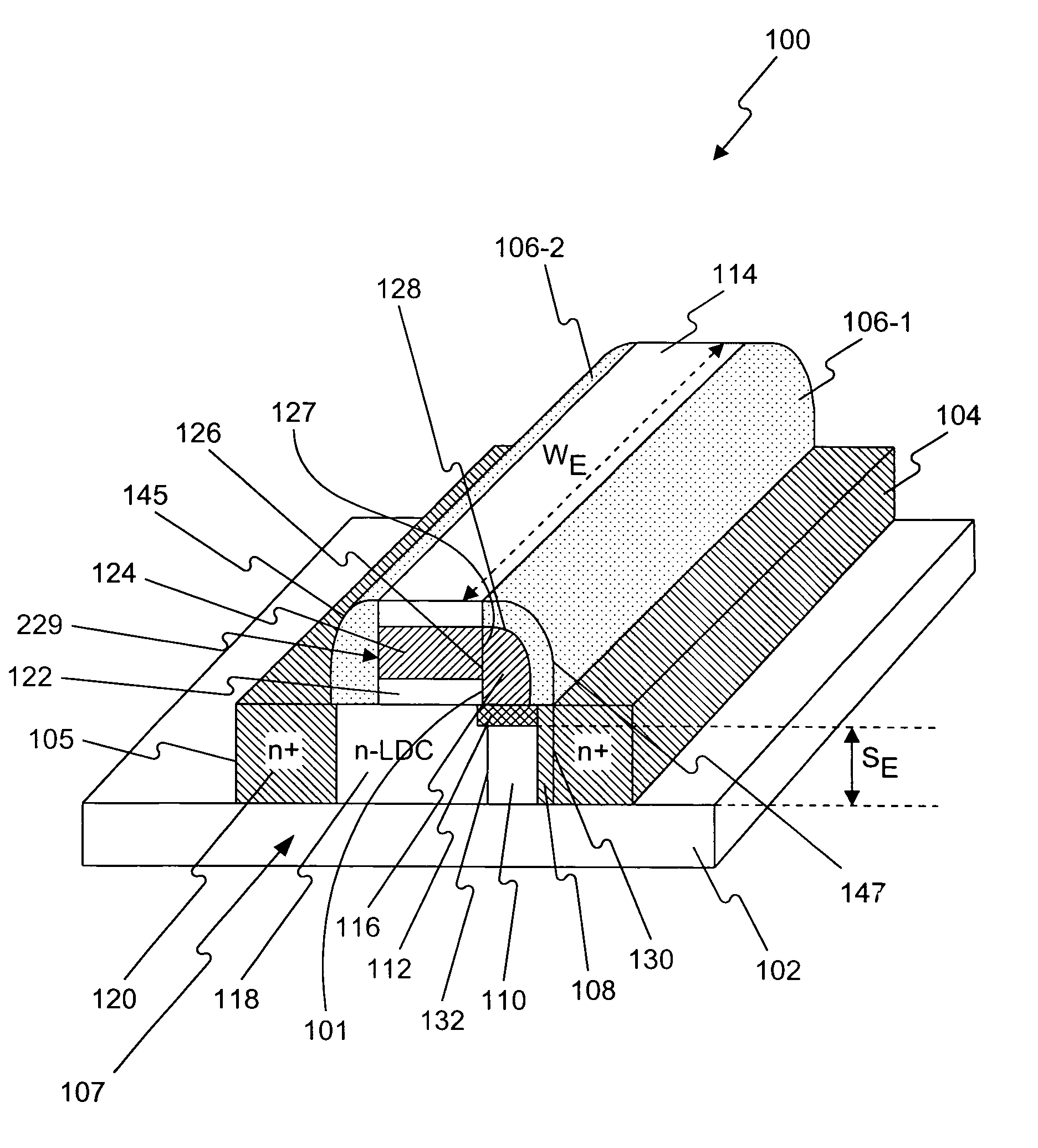
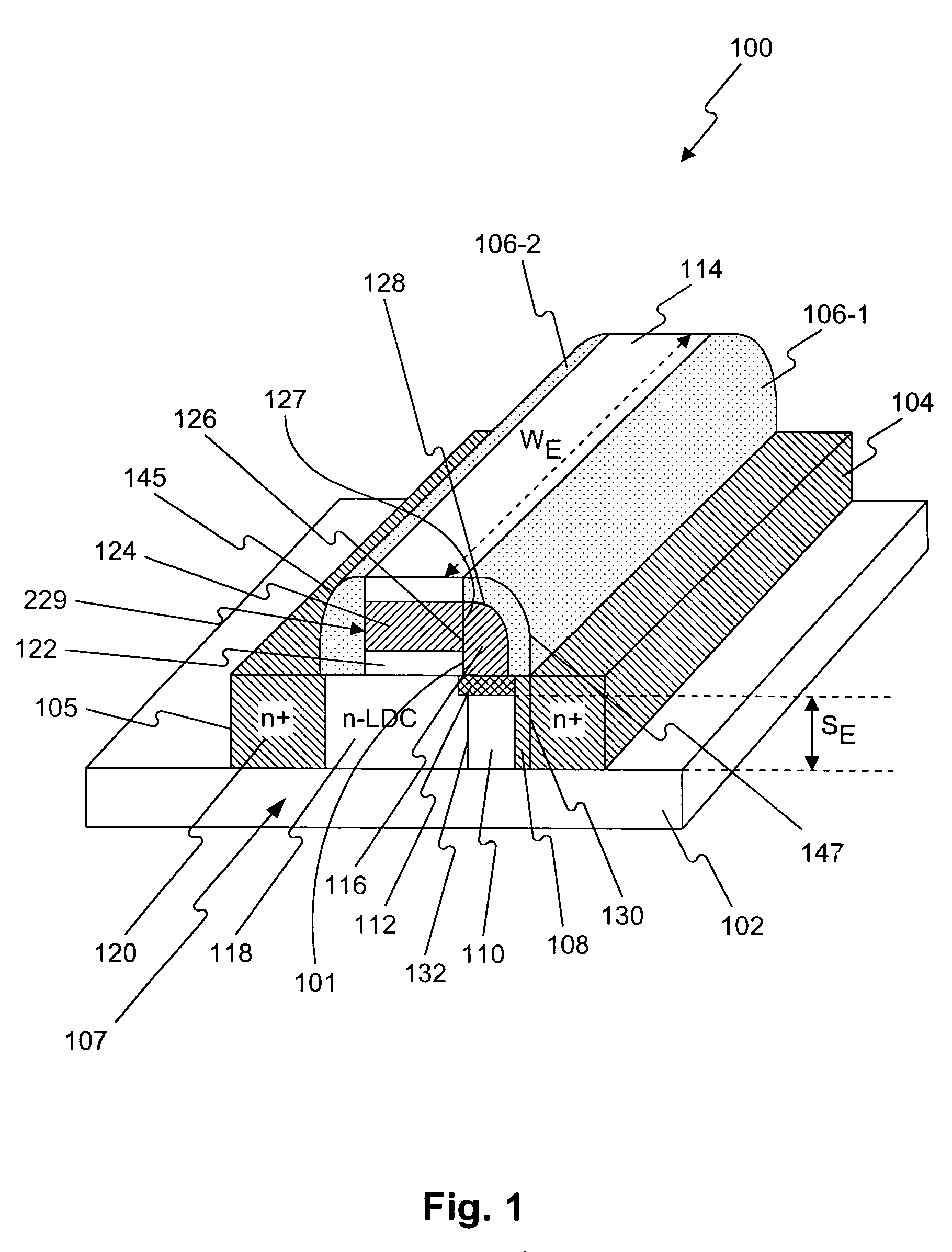
[0029] Consistent with an aspect of the present invention, a lateral bipolar transistor is provided that exhibits similar performance as that of high speed vertical bipolar junction transistors. The lateral bipolar transistor includes a polysilicon side-wall-spacer (PSWS) that forms a contact with the base of the transistor, and thus avoids the process step of aligning the contact mask to a relatively thin base region. The side wall spacer allows self-alignment of the base / emitter region, and has reduced base resistance and junction capacitance. Accordingly, improved fτ and fmax. can be achieved. The lateral bipolar transistor consistent with the present invention can be fabricated on the same substrate as SOI-CMOS devices and other CMOS devices such as FinFETs.
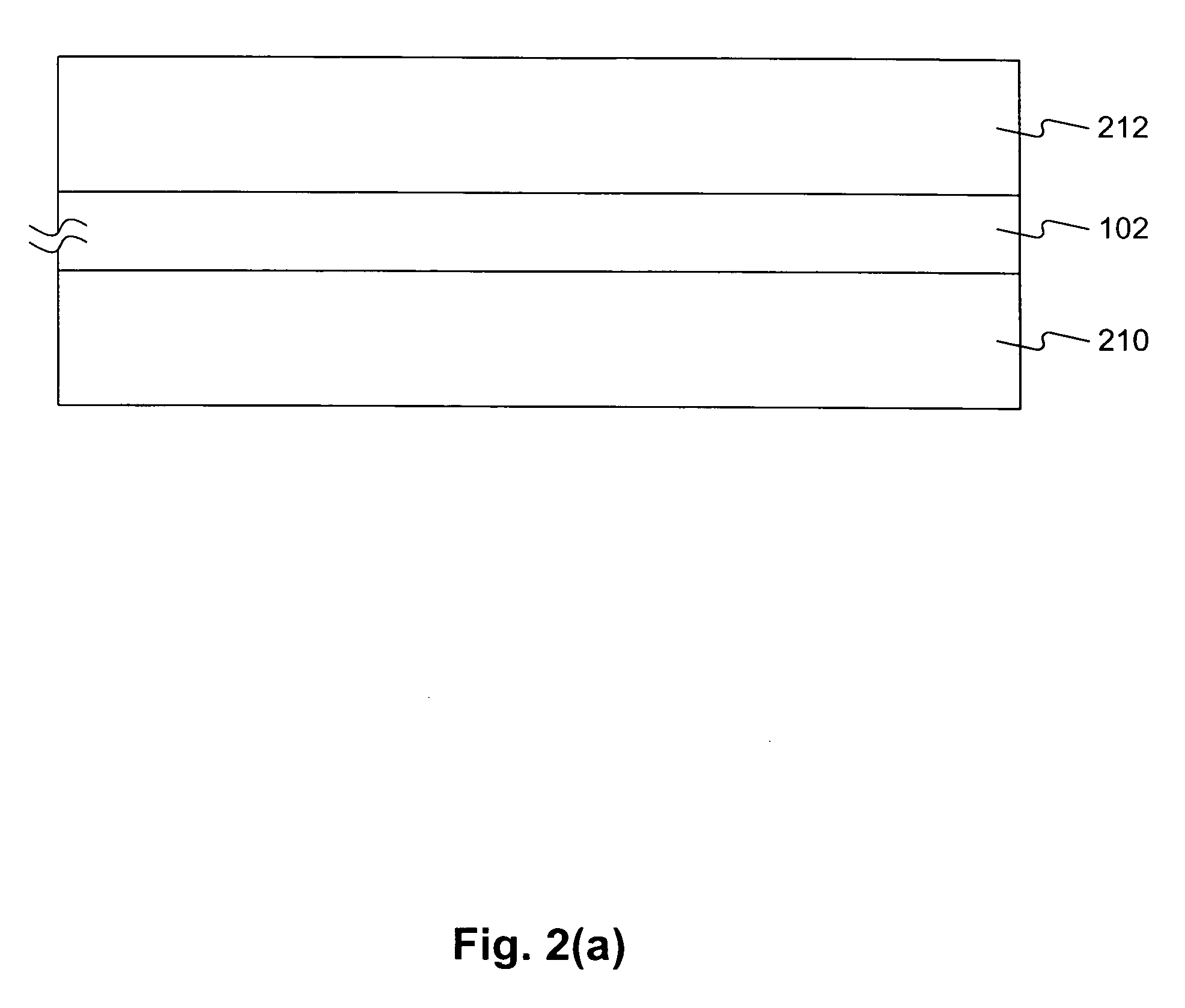
[0030] Reference will now be made in detail to the present preferred embodiments of the invention, examples of which are illustrated in the accompanying drawings. Wherever possible, the same reference numbers will be used th...
PUM
 Abstract
Description
Claims
Application Information