Field emission cold cathode device of lateral type

a cold cathode and field emission technology, applied in the manufacture of electric discharge tubes/lamps, discharge tubes with screens, discharge tubes luminescnet screens, etc., can solve the problems of carbon nanotubes not being oriented well to the extraction electrode, reducing or degrading performance, and exceeding the sharpness of lithography, etc., to achieve low work function

Inactive Publication Date: 2006-03-23
KK TOSHIBA
View PDF22 Cites 26 Cited by
  • Summary
  • Abstract
  • Description
  • Claims
  • Application Information

AI Technical Summary

Problems solved by technology

This is the disadvantage of this device.
When the emitter end face is to be sharpened three-dimensionally, a sharpness exceeding that of the lithography cannot be obtained.
With the method of forming fullerenes or carbon nanotubes by printing, the performance may be decreased or degraded by causes such as high-temperature sintering.
With both bonding and printing, the resulted carbon nanotubes are not oriented well to an extracting electrode, and the problems of an increase in driving voltage, nonuniform electron emission, and the like exist.
With the bonding method, since carbon has a high chemical resistance and is difficult to etch, it is very difficult to pattern carbon to correspond to the cathode interconnection.
This increases the resistance of the interconnection, leading to signal delay or the like.
With the printing method, the film has a high resistance, and it is difficult to form a thick film.
Therefore, a low-resistance interconnection is difficult to form, and signal delay or the like also tends to occur.
The conventionally proposed field emission cold cathode device is, however, not sufficient in terms of sharpness, driving voltage, reliability, yield, manufacturing easiness, and the like.

Method used


Image

  • Field emission cold cathode device of lateral type
  • Field emission cold cathode device of lateral type
  • Field emission cold cathode device of lateral type

Examples


Embodiment Construction

[0035] The embodiments of the present invention will be described with reference to the accompanying drawings. In the following description, constituent elements having substantially the same function and arrangement are denoted by the same reference numerals, and a repetitive description will be made when necessary.

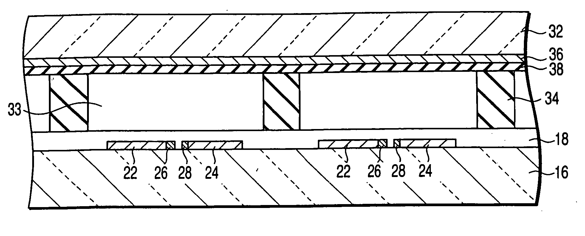
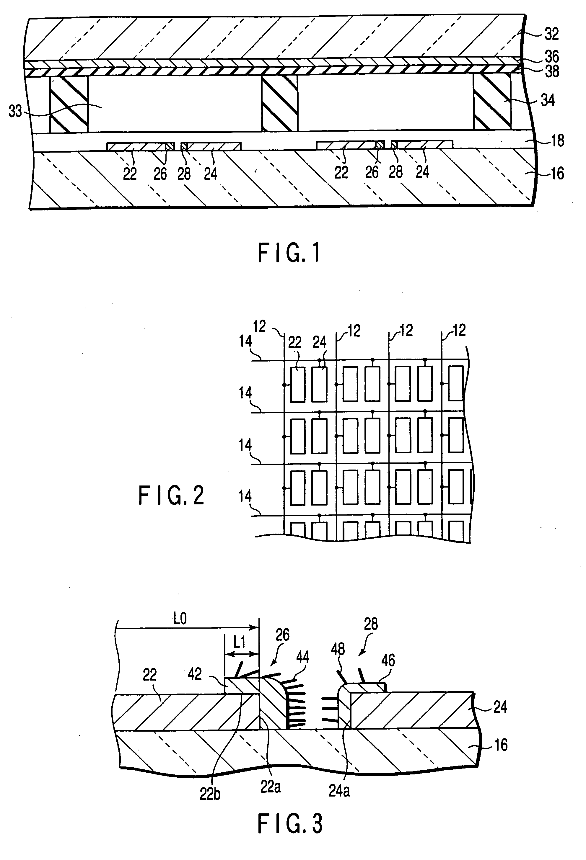
[0036]FIG. 1 is a sectional view showing a flat image display device as an example of a vacuum micro-device to which a field emission cold cathode device of a lateral type according to an embodiment of the present invention is applied. FIG. 2 is a partial plan view of this device, and FIG. 3 is a sectional view of the main part of this device.

[0037] As shown in FIG. 2, this display device has pairs of cathode electrodes 22 and gate electrodes 24 to respectively correspond to a large number of pixels arranged in a matrix. The cathode electrodes 22 are connected to cathode lines 12 running in the vertical direction in FIG. 2, and the gate electrodes 24 are connected to g...


PUM


Abstract

A field emission cold cathode device of a lateral type includes a cathode electrode and gate electrode disposed on a major surface of a support substrate laterally side by side. The cathode electrode and gate electrode have side surfaces which oppose each other, and an emitter is disposed on the opposite side surface of the cathode electrode. The emitter includes a metal plating layer formed on the cathode electrode, and a plurality of granular or rod-shaped micro-bodies. The micro-bodies are consisting essentially of a material selected from the group consisting of fullerenes, carbon nanotubes, graphite, a material with a low work function, a material with a negative electron affinity, and a metal material, and are supported in the metal plating layer in a dispersed state.

Description

CROSS-REFERENCE TO RELATED APPLICATIONS [0001] This application is based upon and claims the benefit of priority from the prior Japanese Patent Application No. 2000-351610, filed Nov. 17, 2000, the entire contents of which are incorporated herein by reference. BACKGROUND OF THE INVENTION [0002] 1. Field of the Invention [0003] The present invention relates to a field emission cold cathode device of a lateral type, a manufacturing method thereof, and a vacuum micro-device. [0004] 2. Description of the Related Art [0005] The present invention relates to a field emission cold cathode device of a lateral type, a manufacturing method thereof, and a vacuum micro-device. [0006] In recent years, a field emission cold cathode device utilizing Si semiconductor processing techniques has been actively developed. As a typical example of such a device, a field emission cold cathode device of a vertical type described by C. A. Spindt et al in Journal of Applied Physics, Vol. 47, 5248 (1976) is kno...

Claims


Application Information

Patent Timeline
Patent Type & Authority Applications(United States)
IPC IPC(8): H01J63/04H01J1/62H01J1/05H01J1/30H01J1/14H01J1/304H01J9/02H01J29/04H01J31/12
CPCB82Y10/00B82Y30/00H01J1/304H01J1/3048Y10S977/939H01J2201/30446H01J2201/30469H01J2329/00H01J9/025C01B32/05H01J1/30
Inventor NAKAMOTO, MASAYUKI
Owner KK TOSHIBA
Why Eureka
Try Eureka