DC bias voltage measurement circuit and plasma CVD apparatus comprising the same
- Summary
- Abstract
- Description
- Claims
- Application Information
AI Technical Summary
Benefits of technology
Problems solved by technology
Method used
Image

Examples
examples
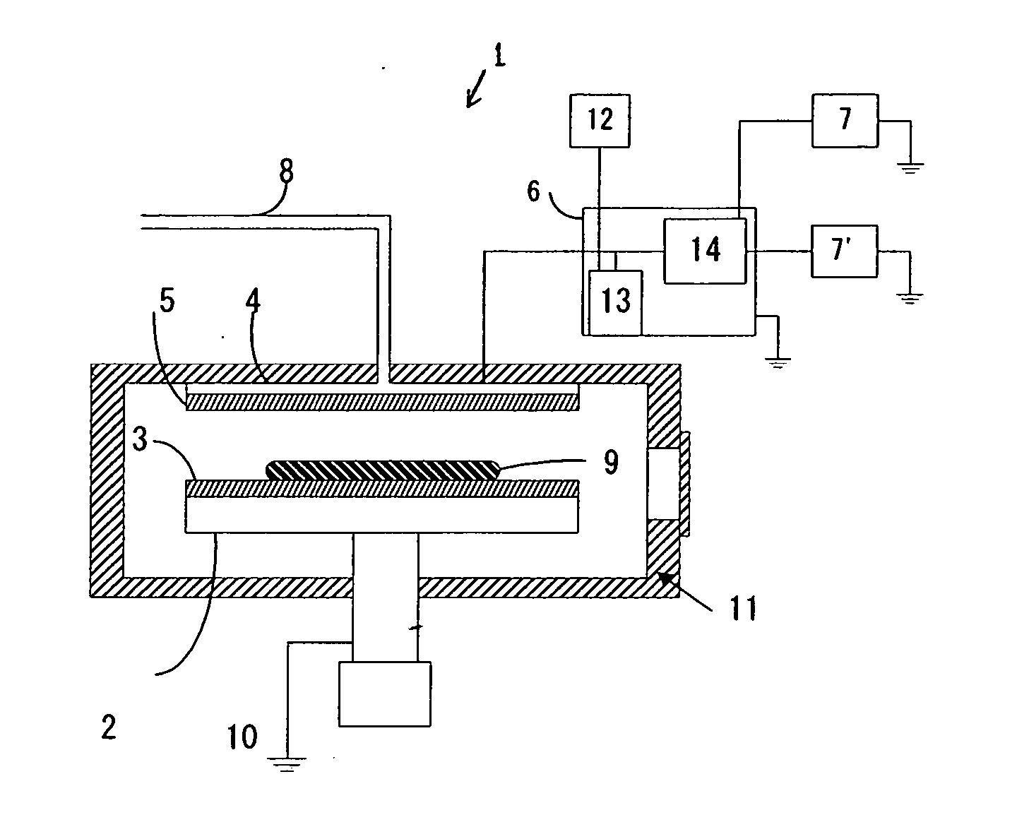
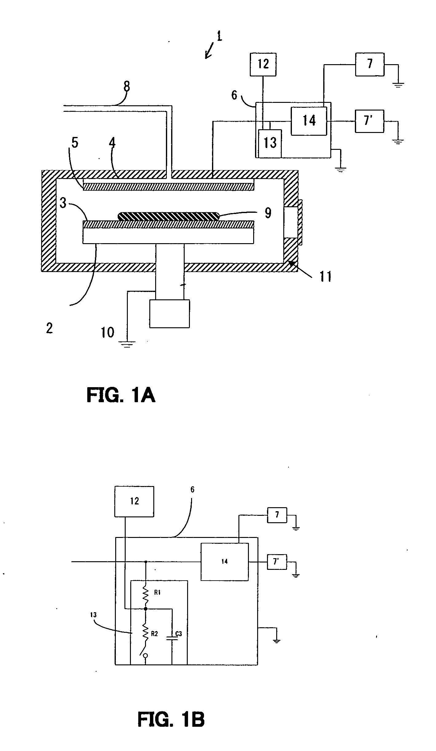
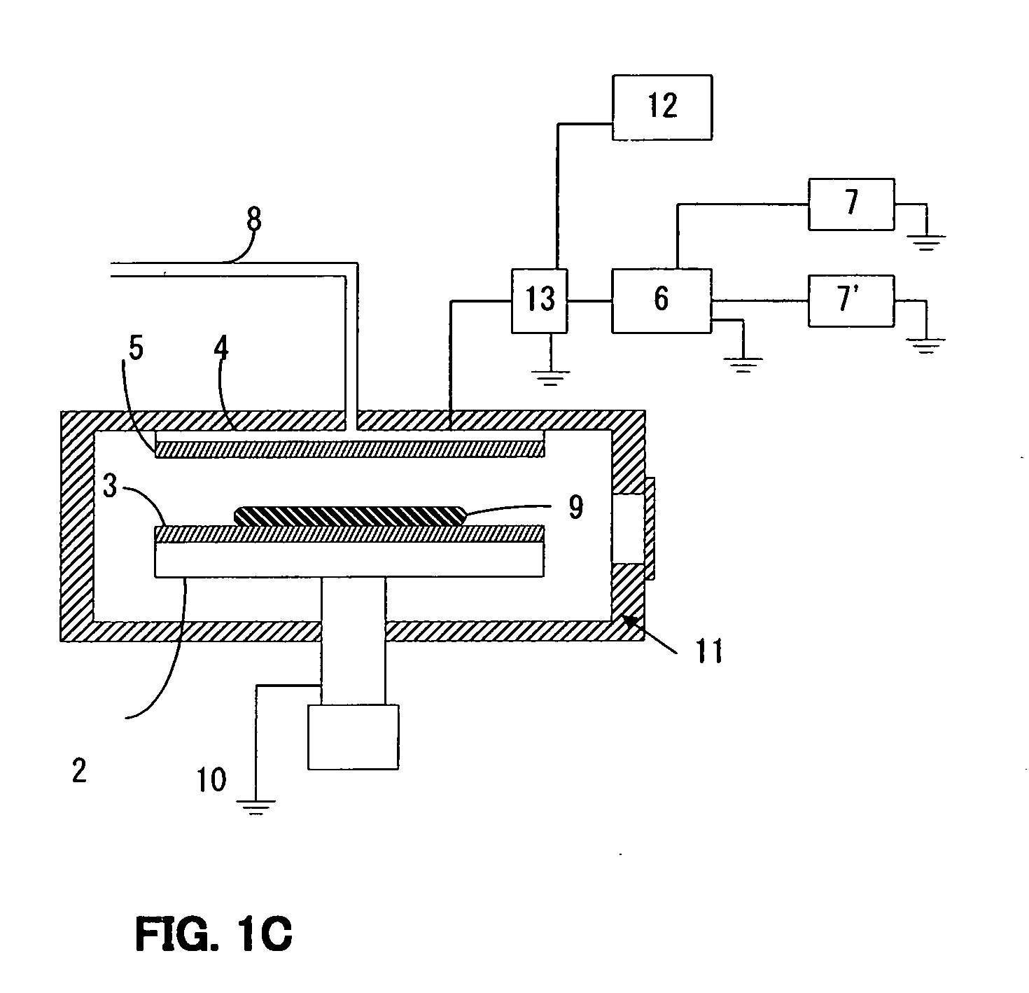
[0060] An input resistance value of the Vdc measurement circuit and occurrence of abnormal discharge are described here in detail with reference to the following examples. The examples are not intended to limit the present invention.
[0061] In the Vdc measurement circuit shown in FIG. 2, an input resistance value means the sum of R1 and R2. An input resistance value used in a conventional Vdc measurement circuit was approx. 1 MΩ. Experiments on whether abnormal discharge occurs or not and how Vm is changed over time when an input resistance value is changed were conducted.
[0062] First, an actual Vdc was measured using an electrostatic field intensity meter. Because measurement using the electrostatic field intensity meter is contactless measurement, it is right to consider that a resistance value is infinitely large. Consequently, a measurement value indicates an actual Vdc value. At this time, abnormal discharge was not observed. Next, Vm change and whether abnormal discharge occu...
PUM
 Abstract
Description
Claims
Application Information
 - R&D
- Intellectual Property
- Life Sciences
- Materials
- Tech Scout
- Unparalleled Data Quality
- Higher Quality Content
- 60% Fewer Hallucinations
Browse by: Latest US Patents, China's latest patents, Technical Efficacy Thesaurus, Application Domain, Technology Topic, Popular Technical Reports.
© 2025 PatSnap. All rights reserved.Legal|Privacy policy|Modern Slavery Act Transparency Statement|Sitemap|About US| Contact US: help@patsnap.com