Fabricating transistor structures for DRAM semiconductor components

a technology of semiconductor components and transistor structures, which is applied in the direction of semiconductor devices, electrical equipment, basic electric elements, etc., can solve the problems of reducing the contact resistance, reducing the data retention time of the dram memory cell, and adversely affecting the dopant profile of the region by heating step, so as to reduce the contact resistance of the cell array without increasing the thermal stress on the implanted structur

Inactive Publication Date: 2006-03-30
INFINEON TECH AG
View PDF9 Cites 16 Cited by
  • Summary
  • Abstract
  • Description
  • Claims
  • Application Information

AI Technical Summary

Benefits of technology

[0020] An object of the invention is to provide a method for fabricating transistor structures for a cell array or for DRAM semiconductor components that allows the contact resistances in the cell array to be reduced without increasing the thermal stresses on implanted structures.
[0021] This and other objects are achieved in accordance with the present invention by providing a method for fabricating transistor structures for cell arrays of DRAM semiconductor components. The method comprises providing gate conductor structures that are spaced apart from each other on a substrate surface of a semiconductor substrate in a cell array such that, between at least two gate conductor structures, first sections of the semiconductor substrate that are to be connected with a CB contact structure and second sections of the semiconductor substrate that are to be connected with a storage capacitor are uncovered in the cell array. A spacer mask is patterned over portions of the substrate including vertical sections along vertical side walls of the gate conductor structures and horizontal sections above the second sections, where the first sections remain uncovered. The method further comprises performing CB implantation of dopants so as to form BC contact regions in the first sections of the semiconductor substrate, activating the dopant of the CB implantation via a high-temperature activation anneal, and depositing silicate glass over portions of the substrate including the gate conductor structures. The deposited silicate glass is partially melted in a reflow heating step, where the reflow heating step is controlled to also facilitate a final furnace anneal that slow anneals lattice defects in the semiconductor substrate.

Problems solved by technology

Each heating step adversely affects the dopant profile of regions that have already been implanted, depending on the maximum temperature and duration of the heating step.
Vacancies or point defects of this type in the crystal lattice promote leakage current mechanisms, which reduce the data retention time of the DRAM memory cell.
Furthermore, the self-aligned formation of metal silicide (saliciding, self-aligned siliciding) is also known to reduce the contact resistance.
For transistor structures with gate widths of less than 100 nanometers, the method described generally exceeds the thermal budget which is permissible for a suitable doping profile.

Method used


Image

  • Fabricating transistor structures for DRAM semiconductor components
  • Fabricating transistor structures for DRAM semiconductor components
  • Fabricating transistor structures for DRAM semiconductor components

Examples


Embodiment Construction

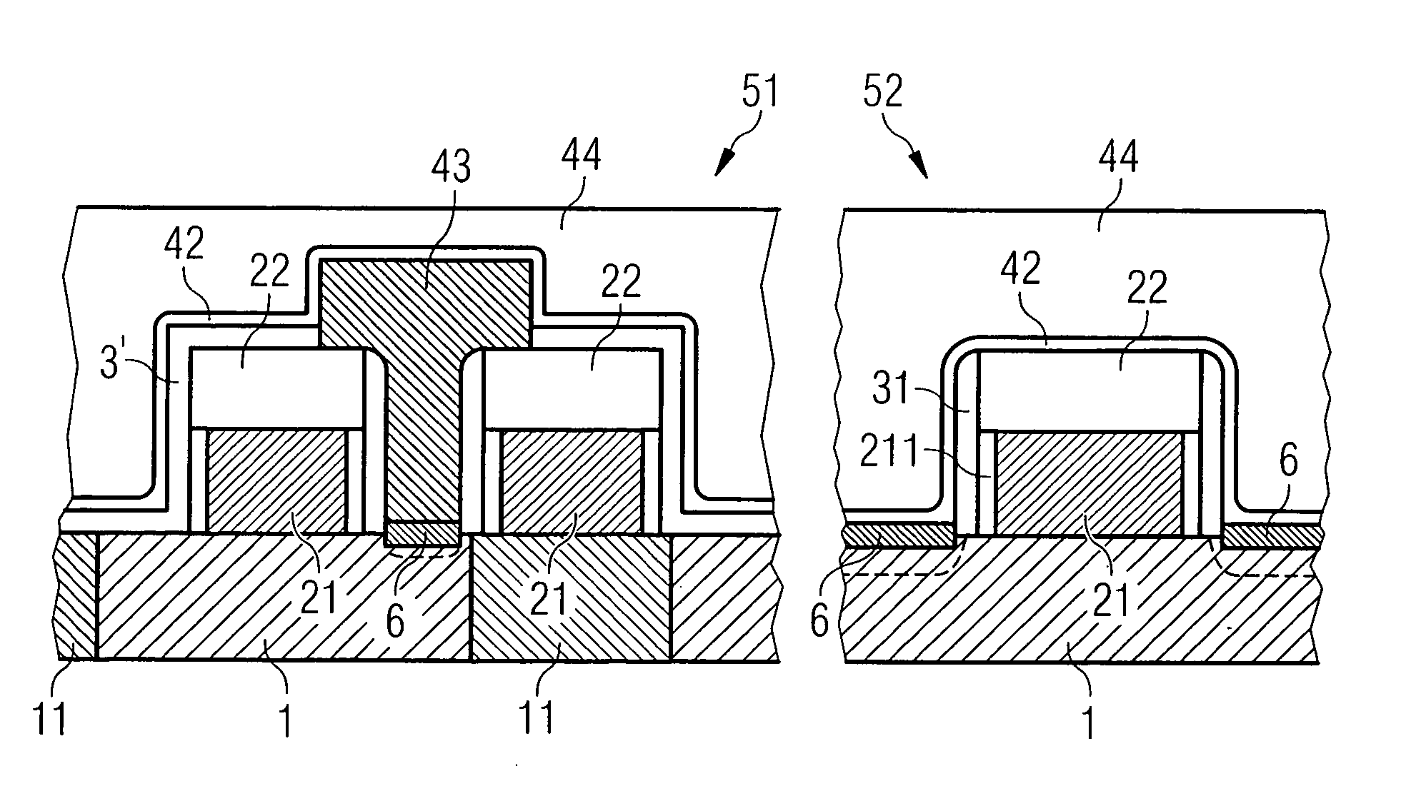
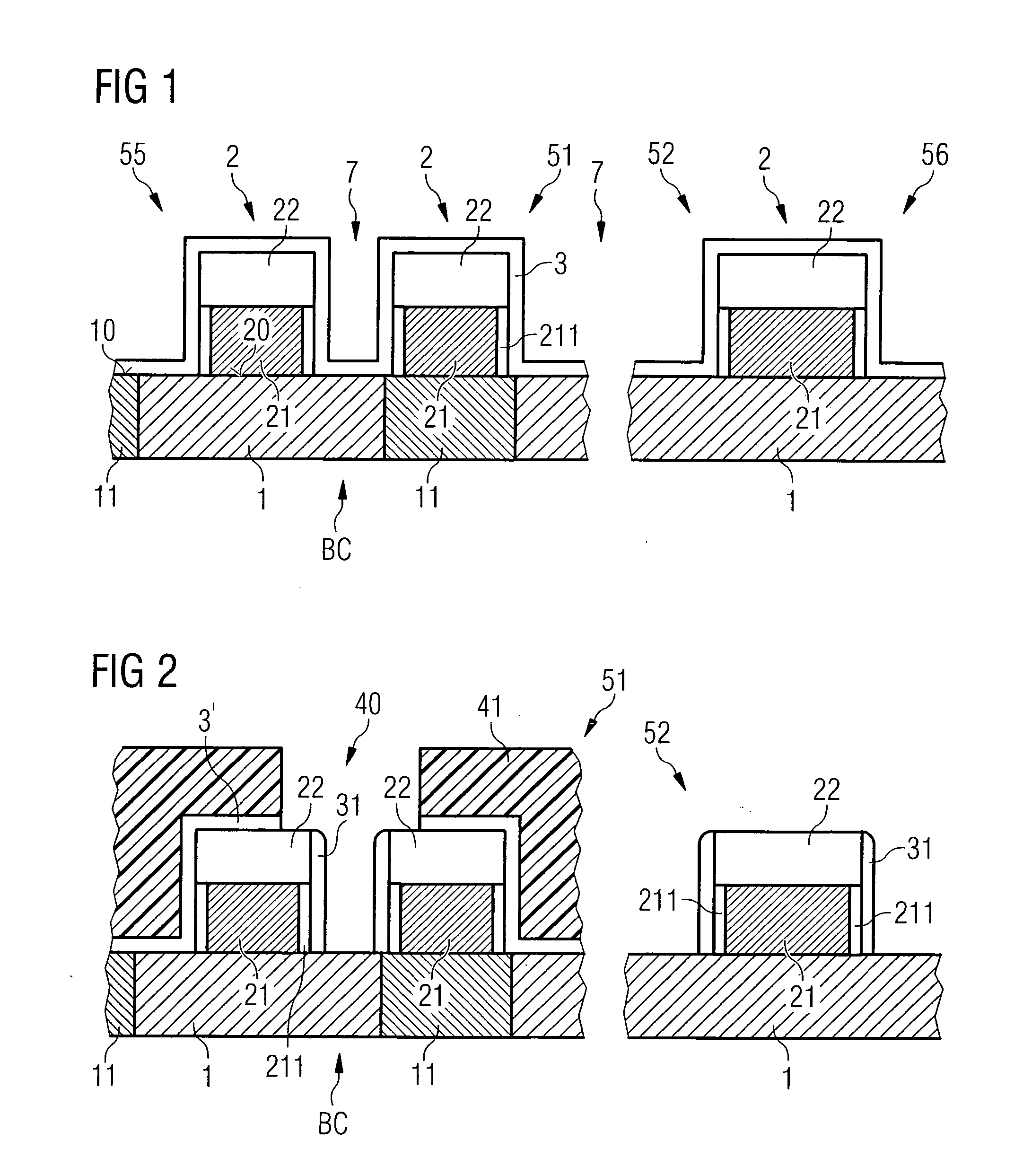
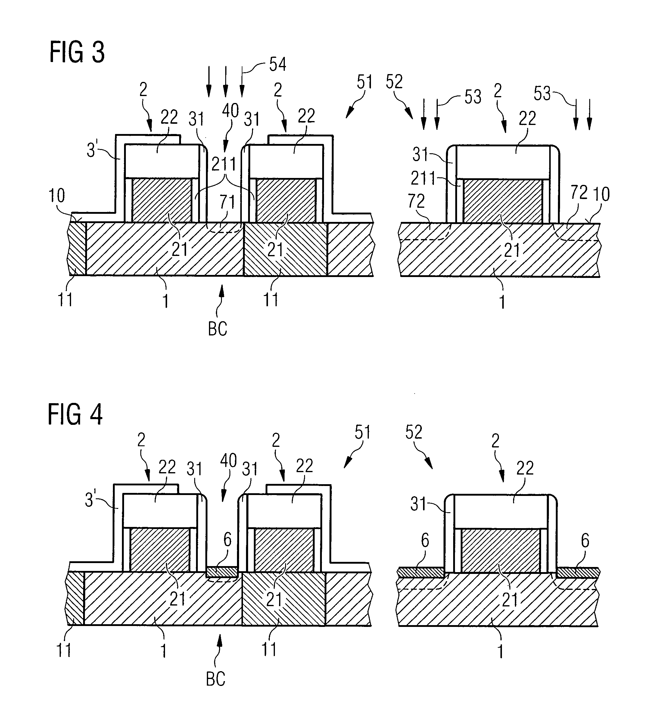
[0025] In accordance with the present invention, a method for fabricating transistor structures for DRAM semiconductor components includes providing gate conductor structures that are spaced apart from one another on a substrate surface of a semiconductor substrate with a cell array. First sections of the semiconductor substrate that connect to a CB contact structure and second sections of the semiconductor substrate that connect to a storage capacitor are uncovered between the gate conductor structures in the cell array. The storage capacitor can be provided as a trench capacitor or as a stack capacitor.

[0026] A spacer mask with vertical and horizontal sections is patterned over the relief on the semiconductor substrate formed from the gate conductor structures. The vertical sections cover the vertical side walls of the gate conductor structures. The horizontal sections of the spacer mask cover the second sections of the semiconductor substrate, with the first sections remaining u...


PUM


Abstract

A method for fabricating transistor structures for DRAM semiconductor components includes forming gate conductor structures in a cell array of a DRAM semiconductor component and covering the structures with a spacer liner. The gate conductor structures lie on a silicon semiconductor substrate. A masked spacer etch produces a spacer mask with horizontal sections and vertical spacer structures from the spacer liner for aligning implantation steps and for self-aligned formation of silicide structures at the surface of the semiconductor substrate. A CB contact implantation step is provided prior to the filling of trenches between the gate conductor structures with dielectric silicate glass fillings, and this obviates the need for an isolated high-temperature activation anneal for the CB contact implantation as well as reducing the thermal stresses on regions of the semiconductor substrate which have already been doped. A reflow heating step for partially melting the silicate glass is controlled as a final furnace anneal for annealing lattice defects in the semiconductor substrate. The contact resistance of a bit contact structure is lowered, while at the same time the thermal stresses are reduced.

Description

CROSS REFERENCE TO RELATED APPLICATIONS [0001] This application claims priority under 35 USC §119 to German Application No. DE 10 2004 047 751.5, filed on Sep. 30, 2004, and titled “Method for Fabricating Transistor Structures for DRAM Semiconductor Components,” the entire contents of which are hereby incorporated by reference. FIELD OF THE INVENTION [0002] The invention relates to fabricating transistor structures for cell arrays of DRAM semiconductor components and to fabricating transistor structures for DRAM semiconductor components. BACKGROUND [0003] DRAM semiconductor components include a cell array in which DRAM memory cells for storing an electric charge that characterizes a data content of the respective memory cell are arranged in a high density and a supporting circuit region or support region including electronic circuits for addressing individual memory cells and for signal conditioning. [0004] The DRAM memory cells each include a storage capacitor for storing the elect...

Claims


Application Information

Patent Timeline
Patent Type & Authority Applications(United States)
IPC IPC(8): H01L21/8242H01L21/20
CPCH01L21/76831H01L21/76897H01L27/10888H01L27/10873H01L27/10855H10B12/05H10B12/485H10B12/0335
Inventor GOLDBACH, MATTHIAS
Owner INFINEON TECH AG
Why Eureka
Try Eureka