Source for thermal physical vapor deposition of organic electroluminescent layers

a technology of thermal physical vapor and electroluminescent layers, which is applied in the direction of electroluminescent light sources, vacuum evaporation coatings, coatings, etc., can solve the problems of failure of electronic devices, and inability to meet the requirements of us

Inactive Publication Date: 2006-04-06
LG DISPLAY CO LTD
View PDF14 Cites 3 Cited by
  • Summary
  • Abstract
  • Description
  • Claims
  • Application Information

AI Technical Summary

Benefits of technology

[0021] An object of the present invention is to provide the deposition source which can compensate change of the distance between the heating means and the surface of the deposition material caused by decrease of the thickness of the deposition material according to consumption of the deposition material in the deposition process for the purpose of solving problems caused by increase of the distance between the top plate (heating means) of the deposition source and the surface of the deposition material supplied into the deposition source from the deposition process.
[0022] Another object of the present invention is to provide the deposition source which can enhance thermal efficiency through preventing heat generated at the heating means from exiting to the exterior by adding a heat-cutting function.
[0023] Further, another object of the present invention is to provide the deposition source for forming organic electroluminescent layers which can obtain a uniform deposition layer by minimizing factors of temperature change and by efficiently using all the deposition material through supplying heat to the deposition source adjoining the surface of the bottom wall.

Problems solved by technology

Organic powder has been recognized as giving a number of disadvantages for this type of thermal vaporization coating.
First, many organics are relatively complex compounds (high molecular weight) with relatively weak bonding, and so intensive care must be taken to avoid decomposition during the vaporization process.
Second, the powder form can give rise to particles of non-vaporized electroluminescent materials.
The particles leave the deposition source with vapor and are deposited as undesirable lumps on the substrate.
These unwanted particulates or droplets may result in unacceptable defects in products, particularly in electronic or optical products, dark spots may appear in images, or shorts or opens may result in failures within electronic devices.
Low molecule organic electroluminescent material contains a large amount of organic material unstable to heat, and causes a problem of lowering the characteristics of the organic electroluminescent material by inducing resolution or change of the material characteristics due to excessive radiant heat in the deposition process.
Such additional processes cause loss of the process time.
Another drawback of the deposition source 10 is that the heat generated at the top plate 11A and the side wall 11D is not sufficiently transferred to the deposition material 20 located at the lower portion of the deposition source 10, that is, the deposition material 20 adjoining the surface of the bottom wall 11E.
Therefore, it is difficult to form a uniform deposition layer on the substrate.

Method used


Image

  • Source for thermal physical vapor deposition of organic electroluminescent layers
  • Source for thermal physical vapor deposition of organic electroluminescent layers
  • Source for thermal physical vapor deposition of organic electroluminescent layers

Examples


first embodiment

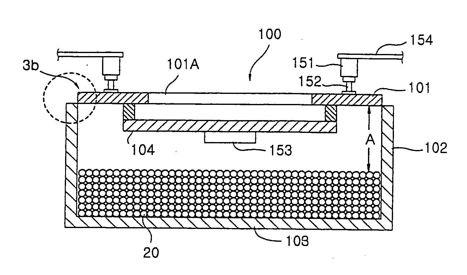
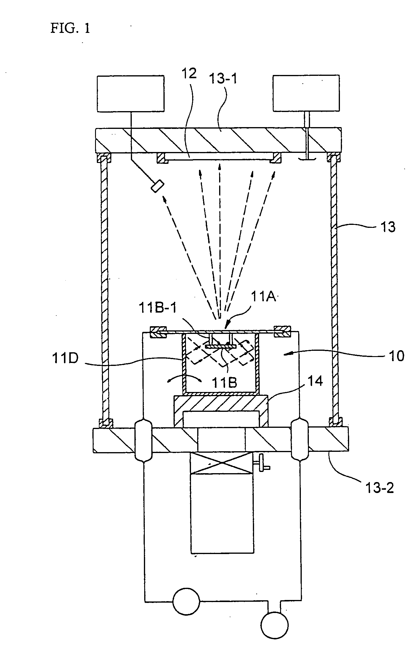
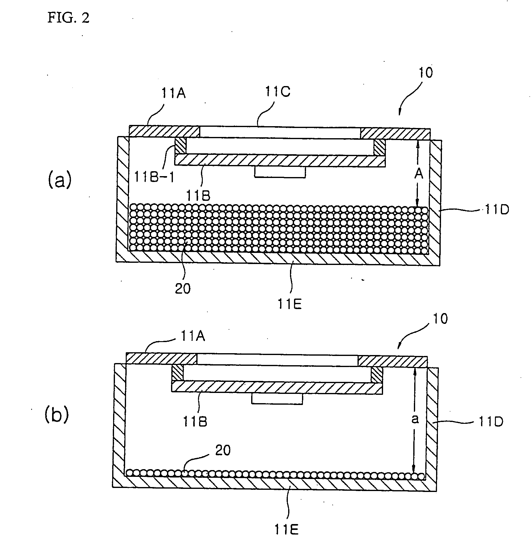
[0041]FIG. 3a is a sectional view of the deposition source according to the first embodiment of the present invention. A deposition source 100 according to the first embodiment is a vessel consisted of a top plate 101, a side wall 102, and a bottom wall 103. The deposition source 100 contains solid organic electroluminescent vapor deposition material 20 (hereinafter, referred to as “deposition material”). A vapor efflux aperture 101A is formed on the top plate 101. The function of the vapor efflux aperture 101A is to discharge vapor of vaporized deposition material from the deposition source 100. A baffle member 104 fixed to a lower surface of the top plate 101 corresponds to the efflux aperture 101A.

[0042] The top plate 101 can act as a heating means (heater) for supplying heat to the deposition material 20 or a separate heating means can be placed on (or below) the top plate 101. In the description below, a case where the top plate 101 acts as a heating means will be explained as...

second embodiment

[0055]FIG. 4 is a sectional view of the deposition source according to the second embodiment of the present invention. The entire structure of a deposition source 200 according to this embodiment is the same as that of the deposition source 100 shown in FIG. 3a and FIG. 3c. In this embodiment, a top plate 201 can act as a heating means (heater) for supplying heat to the deposition material 20 or a separate heating means can be placed on (or below) the top plate 201. In the description below, a case where the top plate 201 acts as a heating means will be explained as an example.

[0056] The most important feature of the deposition source 200 according to the second embodiment is that a bottom plate 203 can be moved vertically in response to change of the distance between the surface of the deposition material 20 and the top plate 201.

[0057] As described above, the uniformity of the deposition layer to be formed on the surface of the substrate (12 in FIG. 1) depends on change of the d...

third embodiment

[0071]FIG. 5 is a sectional view of the deposition source according to the third embodiment of the present invention. The deposition source 300 according to this embodiment has a vessel consisted of a top plate 301 acting as the heating means, a side wall 302, and a bottom wall 303. The structure of the top plate 301, on which a vapor efflux aperture 301A is formed and to which a baffle member 304 is fixed, is the same as the top plates 101 and 201 of the deposition sources 100 and 200 of the first and second embodiments, respectively. Therefore, a further detailed description thereon is omitted.

[0072] The important aspect of the deposition source 300 shown in FIG. 5 is that a number of coils C1, C2, . . . Cn as a heating means for transferring heat to the deposition material 20 are wound around the side wall 302, and a casing 350 is located at the outer side of the side wall 302.

[0073] A number of coils C1, C2, . . . Cn are wound on the outer circumference surface of the side wal...


PUM

PropertyMeasurementUnit
surface areaaaaaaaaaaa
lengthaaaaaaaaaa
widthaaaaaaaaaa

Abstract

The present invention disclosed the deposition source installed in a chamber, heated by applied electric power to transfer heat to a vapor deposition material received therein and applying a vaporized deposition material generated therein to a substrate to form deposition organic electroluminescent layers onto the substrate, and comprising a vessel consisted of a top plate on which a vapor efflux aperture is formed, a side wall, and a bottom wall; a heating means for supplying heat to the deposition material received in the vessel, the heating means being capable of moving vertically; and a means for moving the heating means (or the bottom wall), the moving means (or the bottom wall) being operated in response to the signal of a sensing means on varied distances between the heating means and the surface of said deposition material. Thus, the heating means is moved downward (or the bottom wall) is moved upward by the moving means to maintain the distance between the heating means (or the substrate to be coated) and the surface of the deposition material at an initially-set value when the thickness of the deposition material is decreased.

Description

FIELD OF THE INVENTION [0001] The present invention relates to a deposition source for thermal physical vapor deposition of organic electroluminescent layers, and particularly to a deposition source capable of forming a uniform electroluminescent layer on the entire surface of a substrate by compensating increase of the distance between a deposition material and a heating means (or the substrate) from change of the thickness of the deposition material. BACKGROUND OF THE INVENTION [0002] Thermal physical vapor deposition process, which is one of the processes for depositing an organic electroluminescent device, is a technique to coat an electroluminescent layer on a substrate in a housing with vaporized deposition material. In the deposition process, the deposition material is heated to the point of vaporization and the vapor of the deposition material is condensed on the substrate to be coated after the deposition material is moved out of the deposition source. This process is carri...

Claims


Application Information

Patent Timeline
Patent Type & Authority Applications(United States)
IPC IPC(8): C23C16/00C23C14/12H05B33/10C23C14/24C23C14/26C23C14/54H01L51/50
CPCC23C14/12C23C14/243C23C14/543H01L51/56H10K71/00
Inventor KIM, KI BEOMHAN, YOON SOOTAK, YOON HEUNG
Owner LG DISPLAY CO LTD
Why Eureka
Try Eureka