
Exposure apparatus and device manufacturing method

a manufacturing method and technology of a mask are applied in the field of maskless exposure, which can solve the problems of increasing the mask cost, complex optical system, and difficulty in providing a high throughput and high resolution with a simple structure, and achieves simple structure, high throughput, and high resolution.

Inactive Publication Date: 2006-04-06
CANON KK
View PDF6 Cites 14 Cited by
  • Summary
  • Abstract
  • Description
  • Claims
  • Application Information

AI Technical Summary

Benefits of technology

The present invention provides an exposure apparatus with high resolving power and throughput using a simple structure. The apparatus includes a beam splitter, a spatial light modulator, a beam coupler, a projection optical system, and a controller. The spatial light modulator has a one-dimensional or two-dimensional arrangement of pixels, each pixel having multiple reflective elements that displace in the same direction simultaneously. The device manufacturing method involves exposing an object using the exposure apparatus and then developing the exposed object. The invention can be used in the manufacturing of semiconductor chips, CCDs, LCDs, magnetic sensors, thin film magnetic heads, and other devices.

Problems solved by technology

However, as finer processing to the mask pattern and larger mask sizes are demanded with the improved integration and increased area of the device, an increase of the mask cost becomes problematic.
Disadvantageously, the conventional maskless exposure that utilizes the phase-modulation type SLM has difficulties in providing a high throughput and a high resolution with a simple structure.
A large Schlieren optics is needed to convert a light phase pattern into a light intensity pattern and project the light intensity pattern onto the substrate (U.S. Pat. Nos. 5,486,851 and 6,133,986), but use of the Schlieren optics makes complex the optical system.
In addition, a fine lens array is needed in addition to the Schlieren optics (U.S. Pat. No. 6,133,986), and it is difficult to manufacture and mount the fine lens array having excellent imaging performance with small aberrations and dispersions.

Method used


Image

  • Exposure apparatus and device manufacturing method
  • Exposure apparatus and device manufacturing method
  • Exposure apparatus and device manufacturing method

Examples


first embodiment

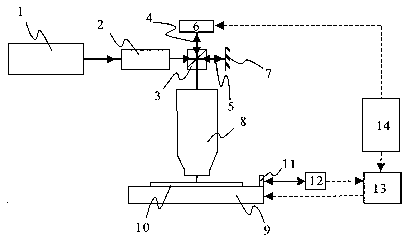
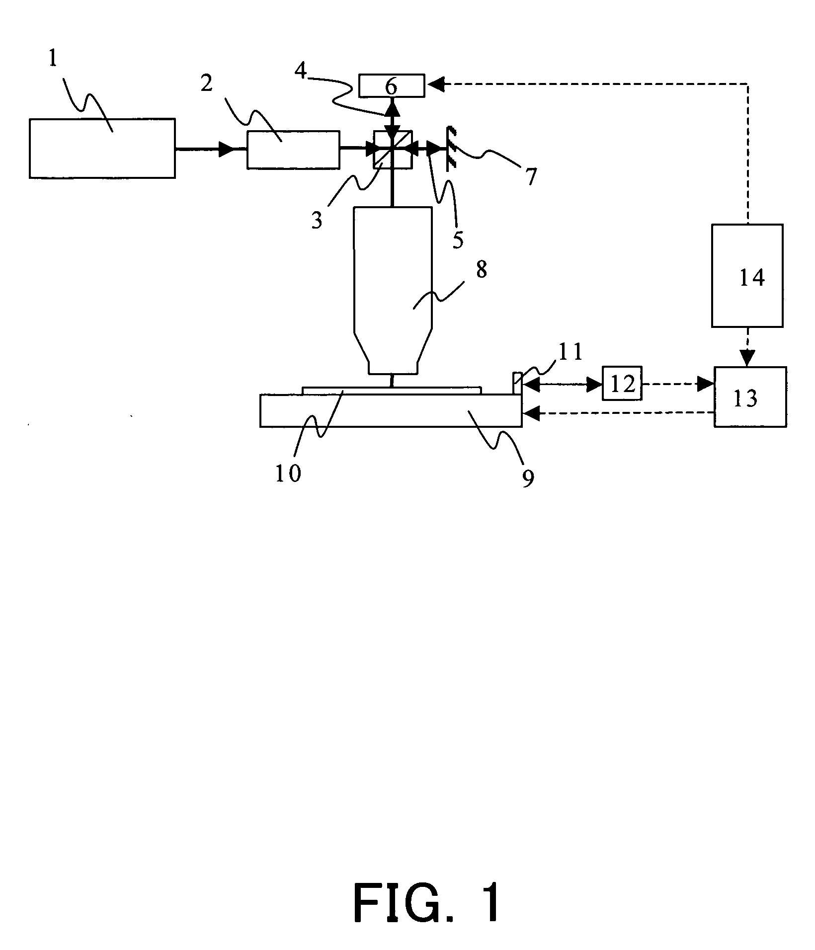
[0019]FIG. 1 is a schematic block diagram of principal part of a maskless projection exposure apparatus according to the present invention. The maskless projection exposure apparatus uses a Michelson's interferometer, which makes a beam splitter and a beam coupler of the same optical element.

[0020] In FIG. 1, 1 denotes a light source, such as a mercury lamp, an excimer laser, a solid laser and a semiconductor laser. An illumination optical system 2 adjusts a beam shape, a polarization state, and a light intensity of the light emitted from the light source 1. The illumination optical system 2 is designed to incorporate known optical elements, such as a lens, a mirror and a polarization element, in accordance with the characteristic of the light source.

[0021] The light from the illumination optical system 2 is incident upon a beam splitter / coupler 3, which divides the light into signal (or first) light 4 and reference (or second) light 5. The beam splitter / coupler 3 may, for example,...

fifth embodiment

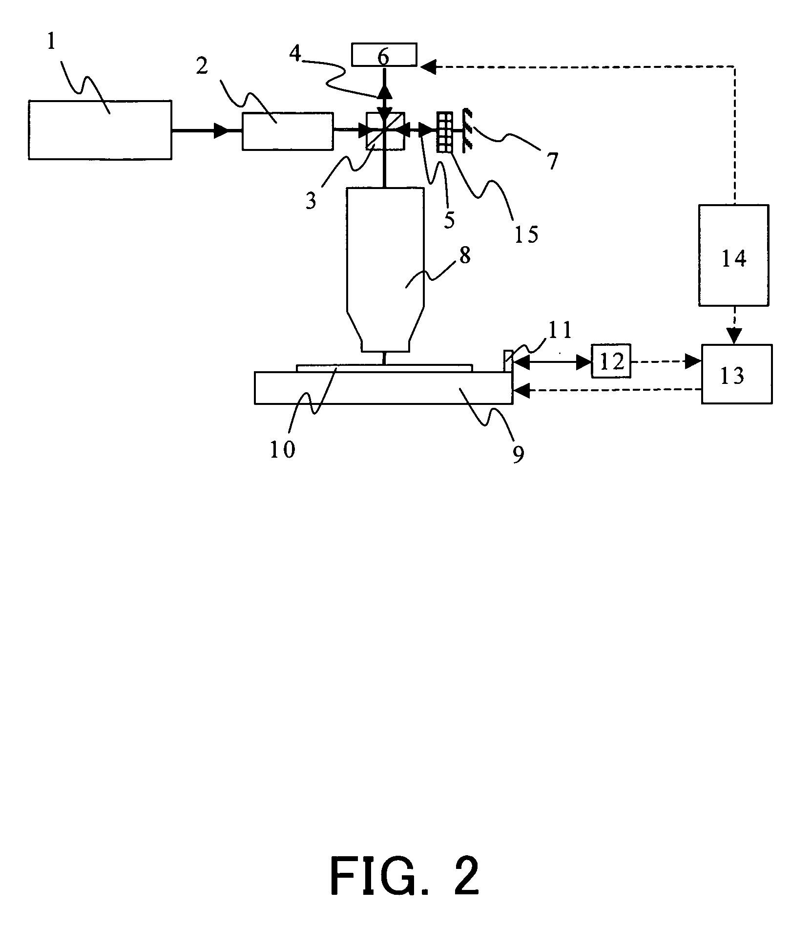
[0039]FIGS. 7 and 8 show an example of the shearing optical system of the In the configuration shown in FIG. 7, after a semi-reflecting mirror 19 (that has a semi-reflecting surface) splits the beam into two, the two beams are reflected on the mirrors 20 and 21, and superimposed on the semi-reflecting mirror 19. The lateral offset amount is adjusted by changing a position of the mirror. In the configuration shown in FIG. 8, a birefringence material 22 splits the beams into two orthogonal polarization directions with a lateral offset between the two beams using the propagation in the birefringence material 22. The birefringence material 22 uses, for example, CaF2 crystal and MgF2 crystal. The shearing optical system that utilizes the birefringence material 22 has an excellent stability due to the common path interferometer, and is suitable for the inventive maskless projection exposure apparatus.

[0040] The fifth embodiment that utilizes the shearing interference optical system may m...


PUM


Abstract

An exposure apparatus includes a beam splitter for splitting light from a light source into first and second beams, a spatial light modulator, arranged in an optical path for the first beam, for modulating a phase distribution of the first beam, a beam coupler for coupling the first beam with the second beam, a projection optical system for projecting a pattern of the spatial light modulator onto a substrate using light from the beam coupler, and a controller for supplying a modulation signal to the spatial light modulator, wherein the spatial light modulator has a one-dimensionally or two-dimensionally arranged pixels, each pixel has plural reflective elements, and the reflective elements in the same pixel displace in the same direction simultaneously.

Description

BACKGROUND OF THE INVENTION [0001] The present invention relates to maskless exposure that forms a pattern on a photosensitive agent applied substrate and manufactures highly integrated devices. The present invention is applicable to manufacturing of a semiconductor device (such as an IC), an imaging device (such as a CCD), a communication device (such as an optical waveguide, and a magnetic head. [0002] A projection exposure apparatus has been conventionally used to expose a mask pattern onto a substrate on which a photosensitive agent is applied, so as to manufacture a semiconductor device, a liquid crystal panel, and the like. However, as finer processing to the mask pattern and larger mask sizes are demanded with the improved integration and increased area of the device, an increase of the mask cost becomes problematic. Accordingly, the maskless exposure that dispenses with the mask for exposure has called attentions. [0003] One exemplary, attractive maskless exposure is a metho...

Claims


Application Information

Patent Timeline
Patent Type & Authority Applications(United States)
IPC IPC(8): G03B27/54
CPCG03F7/70291G03F7/70408G03H2001/0482G03H2225/24G03H2225/32
Inventor HONDA, TOKUYUKI
Owner CANON KK
Learn More