Novel optimization for circuit design

a circuit design and optimization technology, applied in the field of circuit design, can solve the problems of complex custom circuit design, physical custom design is not structured and may take a variety of forms, and the gain in performance comes at a cost of complexity of the design process

Active Publication Date: 2006-04-06
SYNOPSYS INC
View PDF4 Cites 19 Cited by
  • Summary
  • Abstract
  • Description
  • Claims
  • Application Information

AI Technical Summary

Benefits of technology

[0032] In still another aspect of the present invention, a method to optimize a circuit using convex optimization with at least one design parameter includes: minimizing an objective function ƒ, wherein the ƒ is posynomial on an exponent of the design parameter; and solving the ƒ to obtain at least one optimized design parameter value.

Problems solved by technology

Custom circuit design is typically far more complex than standard-cell based design.
Further, the physical custom designs are not structured and may take a variety of forms.
However, this gain in performance comes at a cost: complexity of the design process.
Unfortunately, the complexity of the design process has only increased over time.
The problem is exacerbated by a shortage of custom circuit designers, especially analog designers.
Unlike standard cell design, the performance of custom circuit designs are typically very sensitive to small changes in design variables.
The designer must be very precise in determining all of the design variables, or the resulting circuit performance will be poor at best.
Additionally, each design variable using the custom design approach typically affects all the performance indices in a complex, highly nonlinear way.
The designer typically spends a long time tweaking the circuit and trying to obtain the greatest amount of performance possible out of it in light of the constraints within which he or she must work.
Unfortunately, this custom design flow has several disadvantages.
First, the process is extremely time consuming.
In fact, given the choice, designers would spend longer time tweaking the variables on their designs than schedules permit.
Generally, it is very difficult to determine when to stop tweaking a circuit to achieve maximum performance.
The custom design flow does not encapsulate the knowledge of the experienced designer and as such it cannot be used later by a less experienced designer, or even re-used by the experienced designer to modify the existent circuit efficiently.
In particular, even though the type of equations that can be used is restricted (i.e., the equations must be convex) they can still be highly nonlinear and complex and can be used to represent intricate circuit behavior.
Also, infeasibility is unambiguously detected.
That is, if the methods used do not produce a feasible circuit-based solution, they may produce a certificate that proves that the problem is infeasible.
As an illustration, these errors may become significantly pronounced in deep submicron CMOS processes.
The geometric programming method is typically not accurate for transistors having a small channel length, where channel length modulation, body-effect, drain-induced barrier lowering, vertical field mobility degradation, and other non-idealities complicate the equations for the transistor parameters As another example, transistors operating in the subthreshold or weak inversion regions of operation cannot be modeled accurately using geometric programming methods.
Numerous other examples exist in circuit design where design parameters cannot be accurately optimized where the equation-based method is limited to geometric programming form using simple design parameters.
Yet another shortcoming of geometric programming based methods is that general linear constraint functions cannot be used.
In particular, geometric programming is limited to posynomial inequality and monomial equality constraints.
This characteristic of geometric programming results in several practical disadvantages in the realm of circuit design.
These two basic laws which govern almost all analog circuits, however, typically result in posynomial equality constraints, and thus cannot be handled using geometric programming.

Method used


Image

  • Novel optimization for circuit design
  • Novel optimization for circuit design
  • Novel optimization for circuit design

Examples


Embodiment Construction

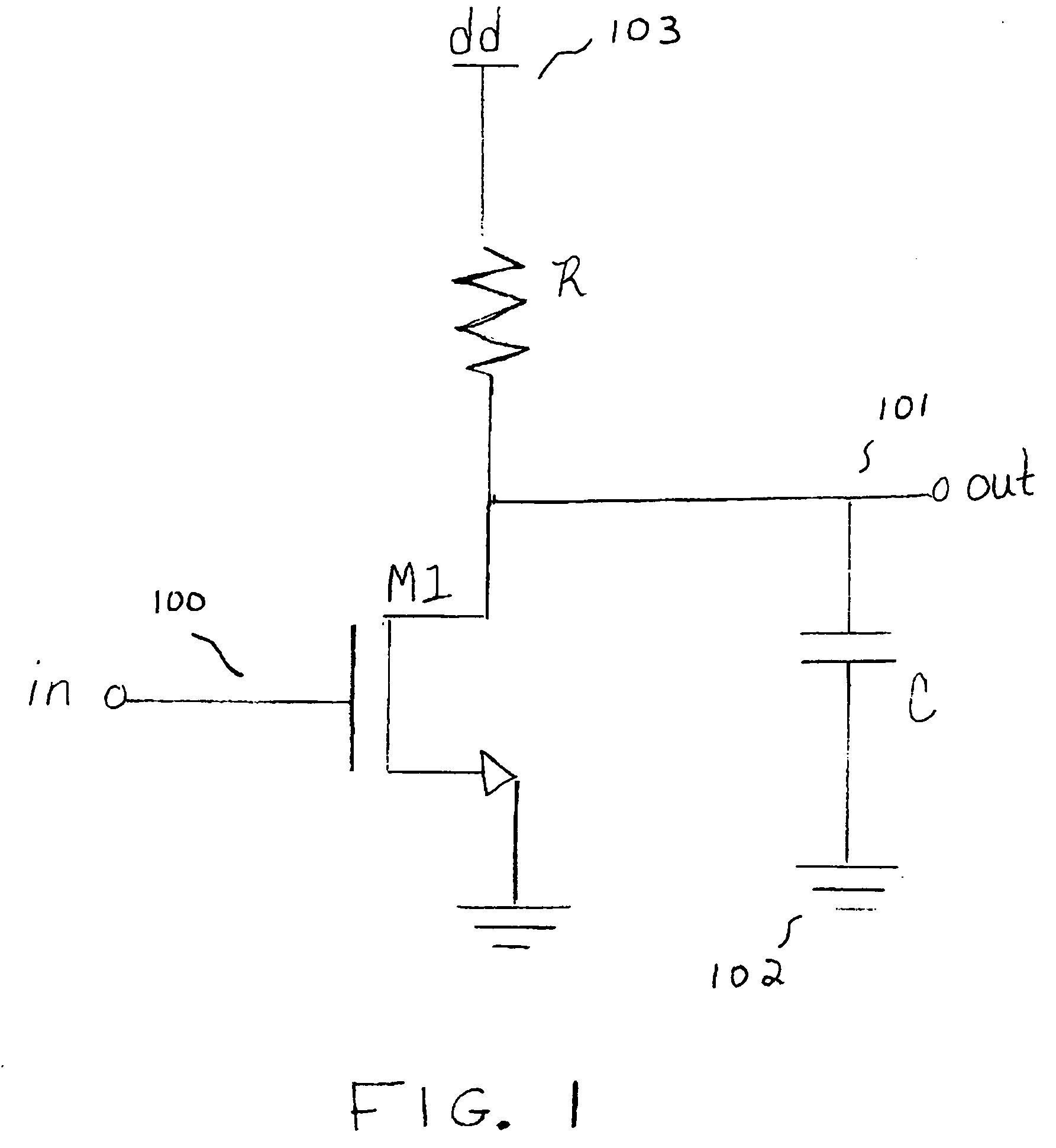
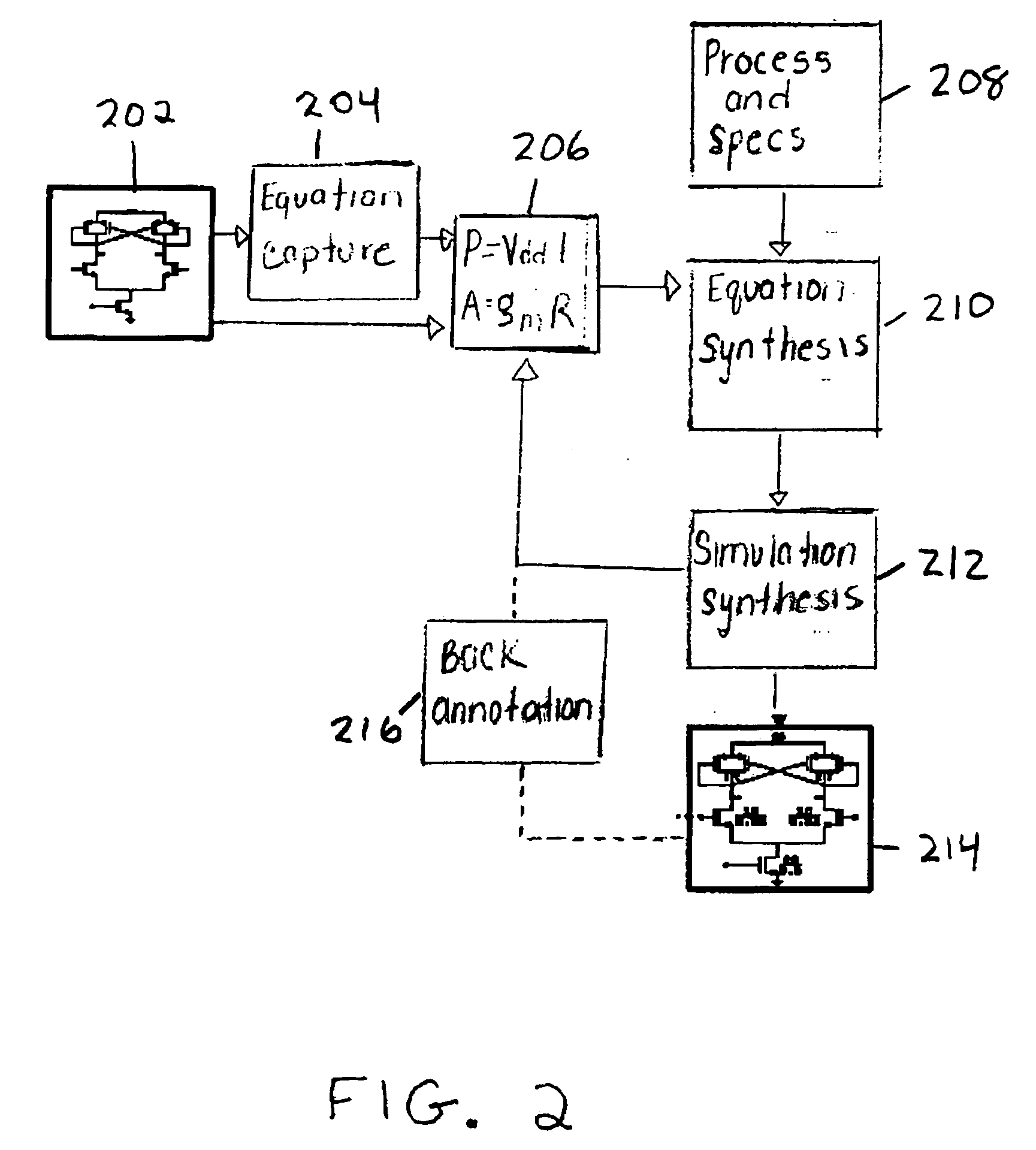
[0047] The detailed description set forth below in connection with the appended drawings is intended as a description of various embodiments of the present invention and is not intended to represent the only embodiments in which the present invention may be practiced. Each embodiment described in this disclosure is provided merely as an example or illustration of the present invention, and should not necessarily be construed as preferred or advantageous over other embodiments. The detailed description includes specific details for the purpose of providing a thorough understanding of the present invention. However, it will be apparent to those skilled in the art that the present invention may be practiced without these specific details. In some instances, well-known structures and devices are shown in block diagram form in order to avoid obscuring the concepts of the present invention.

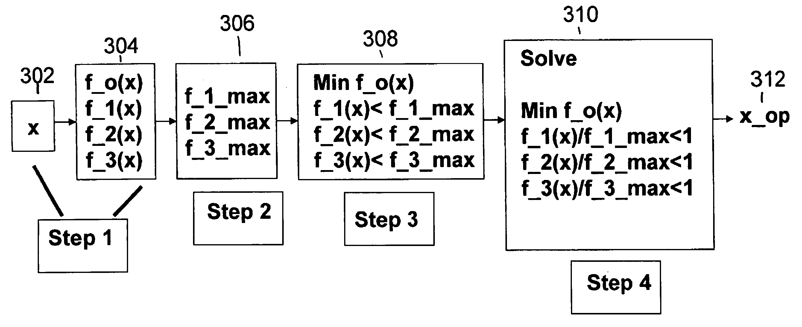
[0048] In one aspect of the present invention, the exponents of design parameters are used. For the...


PUM


Abstract

Methods for optimizing design parameters of a circuit are disclosed. In one aspect, an optimization problem includes one or more performance specifications that represent an exponent of a design parameter to be optimized. Various parameters of passive and active circuit devices may be efficiently and accurately optimized as a result. In another aspect, linear performance specifications are included for accurately calculating voltages. In yet other aspects of the invention, three special types of convex optimization problems are disclosed for enabling the above use of exponents of design parameters which provide efficient and accurate calculations of a virtually unlimited array of circuit parameters and performance characteristics.

Description

RELATED APPLICATION DATA [0001] This application claims priority to U.S. provisional application Ser. No. 60 / 614,745, entitled “Novel Optimization For Circuit Design”, filed Sep. 30, 2004, Mar Hershenson and David M. Colleran, inventors. The content of this provisional application is incorporated by reference as though fully set forth herein.BACKGROUND OF THE INVENTION [0002] 1. Field of Invention [0003] The present invention relates generally to circuit design, and more specifically to methods for designing circuits using equation-based optimization. [0004] 2. Description of Related Art [0005] The need for more efficient and effective equation and software-based methods for integrated circuit design has become paramount for today's businesses involved in the development of electronic and computer devices. Over the last decade, various such methods have been introduced in the arenas of both digital and analog circuit design. As the level of sophistication of electronic devices and t...

Claims


Application Information

Patent Timeline
Patent Type & Authority Applications(United States)
IPC IPC(8): G06F17/50G06F17/10G06F7/60
CPCG06F17/5045G06F17/505G06F17/5063G06F17/5068G06F30/36G06F30/327G06F30/30G06F30/39G06F30/398G06F30/373
Inventor HERSHENSON, MARCOLLERAN, DAVID M.
Owner SYNOPSYS INC
Why Eureka
Try Eureka