Semiconductor device and method for fabricating the same

a semiconductor and device technology, applied in semiconductor devices, capacitors, electrical equipment, etc., can solve the problems of resolution failure, difficult control of the depth of the groove, and opening failure in some of the grooves, so as to increase parasitic capacitance and control the depth of the plate contact more accurately.

Inactive Publication Date: 2006-04-13
PANASONIC CORP
View PDF2 Cites 27 Cited by
  • Summary
  • Abstract
  • Description
  • Claims
  • Application Information

AI Technical Summary

Benefits of technology

[0017] With the foregoing in mind, an object of the present invention is to provide a semiconductor device which can prevent the occurrence of a level difference of an interlayer insulating film between a DRAM regio

Problems solved by technology

Then, when the photoresist 128 is applied onto the third interlayer insulating film 127, the level difference formed on the top of the third interlayer insulating film 127 causes shift of focus, resulting in the occurrence of resolution failure.
As a result, in forming the grooves 143 to 145 in the step shown in FIG. 5, control of the depths of the grooves becomes difficult, which causes a problem that opening failure arises in some of the groov

Method used


Image

  • Semiconductor device and method for fabricating the same
  • Semiconductor device and method for fabricating the same
  • Semiconductor device and method for fabricating the same

Examples


first embodiment

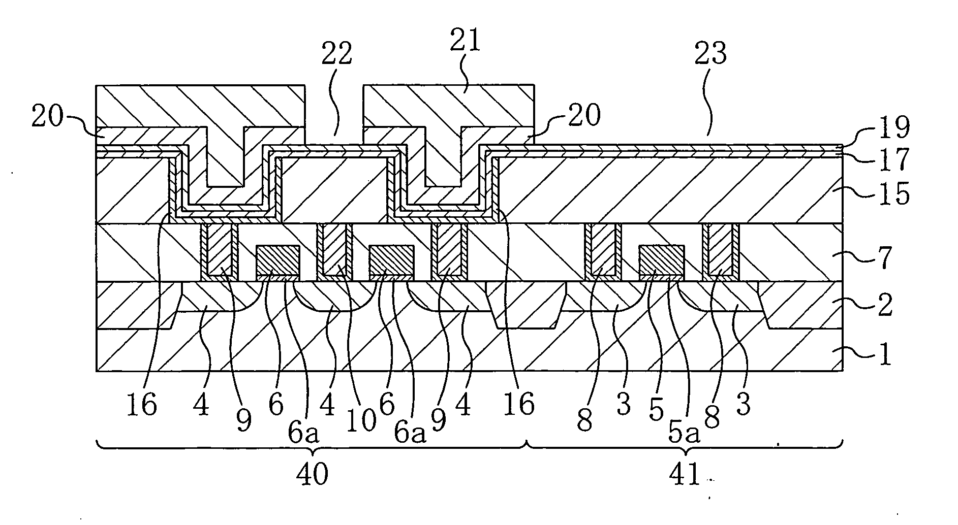
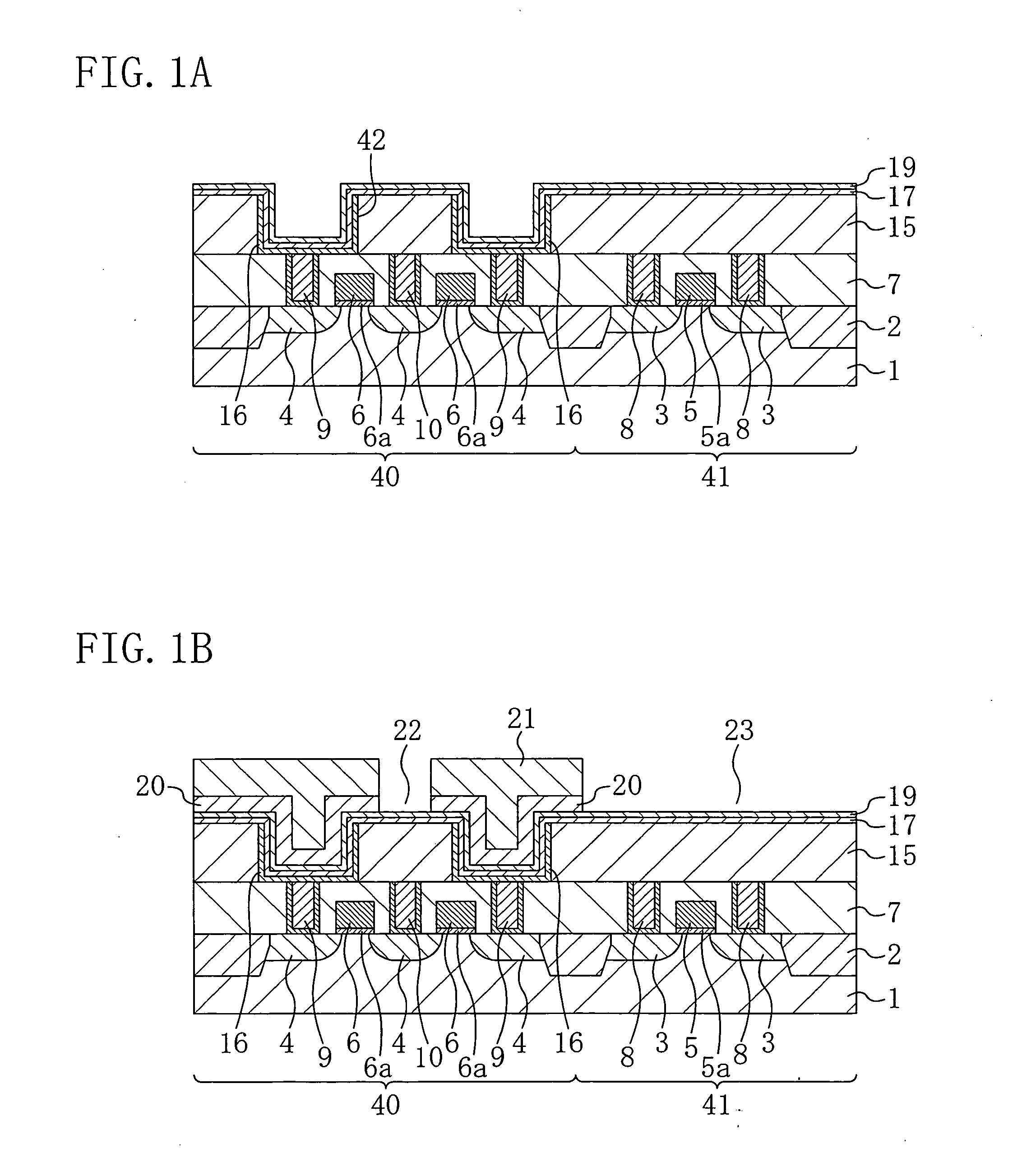
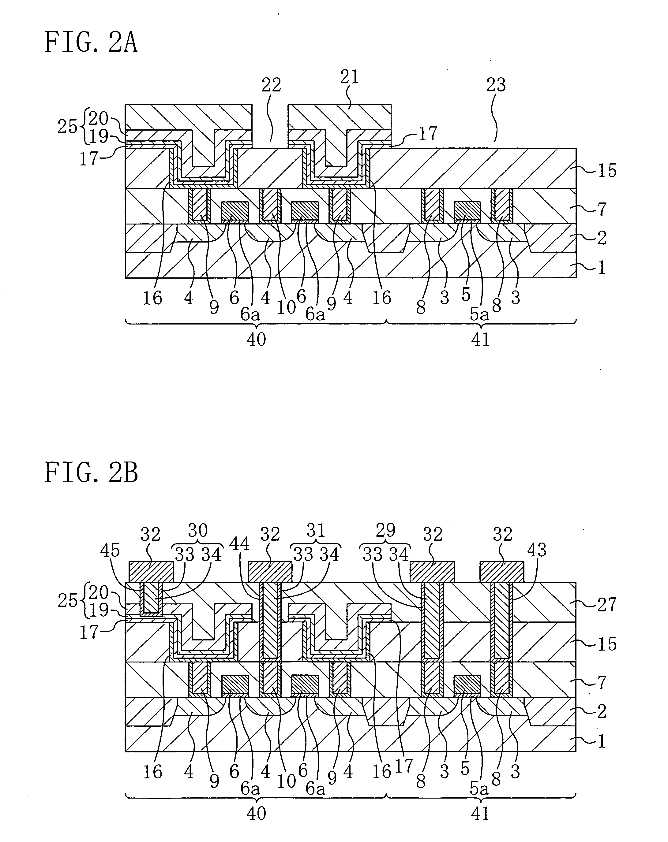
[0038]FIGS. 1A, 1B, 2A, and 2B are sectional views showing fabrication steps of a DRAM-embedded semiconductor device according to a first embodiment of the present invention.

[0039] In the fabrication method of the first embodiment, first, in the step shown in FIG. 1A, an isolation region (STI) 2 is formed in a p-type semiconductor substrate 1. Areas of the p-type semiconductor substrate 1 surrounded with the isolation region 2 are formed with doped source and drain layers 3 and 4, respectively. Above a portion of the p-type semiconductor substrate 1 located in a DRAM region 40, a gate electrode 6 is formed with a gate insulating film 6a interposed therebetween, thereby forming a DRAM memory cell transistor. Above a portion of the p-type semiconductor substrate 1 located in a logic region 41, a gate electrode 5 is formed with a gate insulating film 5a interposed therebetween, thereby forming a logic transistor. Thereafter, a first interlayer insulating film 7 covering the gate elect...


PUM


Abstract

In a method for fabricating a semiconductor device according to the present invention, a groove is formed in a second interlayer insulating film, and then a storage electrode is formed which covers bottom and side surfaces of the groove. A capacitor insulating film is formed on the storage electrode, and a CVD method at a low temperature of 400° C. or lower and annealing with ammonia are repeated to form a TiOxNy film on the capacitor insulating film. A TiN film is formed on the TiOxNy film, and the TiN film is etched using the TiOxNy film as a stopper. The exposed TiOxNy film is then removed to form a plate electrode made of the TiOxNy film and the TiN film.

Description

CROSS-REFERENCE TO RELATED APPLICATIONS [0001] This application claims priority under 35 U.S.C. § 119 on Patent Application No. 2004-297464 filed in Japan on Oct. 12, 2004, the entire contents of which are hereby incorporated by reference. BACKGROUND OF THE INVENTION [0002] (a) Fields of the Invention [0003] The present invention relates to semiconductor devices and methods for fabricating the device. In particular, the present invention relates to DRAM-embedded semiconductor devices (semiconductor devices with DRAMs embedded therein) which have CUB (Capacitor Under Bit-Line) structures, and methods for fabricating such a device. [0004] (b) Description of Related Art [0005] DRAM-embedded LSIs can have data buses of increased width between their memories and logics, and thereby excel in high speed processing of a large amount of data. The DRAM-embedded LSIs also have the property of reducing power consumption of systems therein without requiring any wiring such as a printed wiring bo...

Claims


Application Information

Patent Timeline
IPC IPC(8): H01L29/94
CPCH01L21/31122H01L21/318H01L21/32135H01L27/10811H01L27/10888H01L27/10894H01L28/60H01L21/02271H01L21/02186H10B12/312H10B12/485H10B12/09
Inventor NAKABAYASHI, TAKASHIARAI, HIDEYUKIOHTSUKA, TAKASHIYANO, HISASHI
Owner PANASONIC CORP
Why Eureka
Try Eureka