Structure and method for mounting LSI package onto photoelectric wiring board, information processing apparatus, optical interface, and photoelectric wiring board

a technology for photoelectric wiring and lsi packages, applied in semiconductor lasers, semiconductor/solid-state device details, instruments, etc., can solve the problems of increasing module costs, high maintenance costs, and difficult replacement of components on the maintenance spot, and achieves easy replacement, high precision, and sufficient precision

Inactive Publication Date: 2006-04-13
NEC CORP
View PDF7 Cites 48 Cited by
  • Summary
  • Abstract
  • Description
  • Claims
  • Application Information

AI Technical Summary

Benefits of technology

[0016] In accordance with the present invention, a guide member is mounted on each of a photoelectric wiring board and an optical interface with high precision. Positioning is conducted by fitting these guide members each other. According to the present invention, optical axis alignment between a plurality of optical elements mounted on the optical interface and a optical transmission line can be achieved with sufficient precision without conducting complicated optical axis adjustment work when mounting an LSI package including the optical interface on the photoelectric wiring board.

Problems solved by technology

Therefore, it is difficult to replace components on the maintenance spot for an information processing apparatus.
This is because chip mounting equipment required for component replacement using solder bump melting is not typically installed on the maintenance spot for an information processing apparatus, and consequently it is necessary to bring a board into an assembly factory and replace the optical element or the LSI chip.
A sophisticated processing technique and a sophisticated mounting technique become necess

Method used


Image

  • Structure and method for mounting LSI package onto photoelectric wiring board, information processing apparatus, optical interface, and photoelectric wiring board
  • Structure and method for mounting LSI package onto photoelectric wiring board, information processing apparatus, optical interface, and photoelectric wiring board
  • Structure and method for mounting LSI package onto photoelectric wiring board, information processing apparatus, optical interface, and photoelectric wiring board

Examples


first embodiment

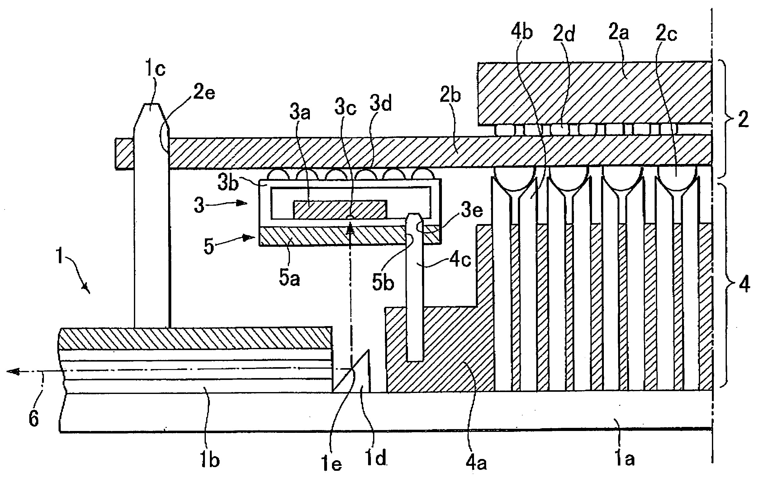
[0026]FIG. 3 is a sectional view showing a structure in a first embodiment according to the present invention. A module in the present embodiment is formed to have bilateral symmetry. Therefore, only the left half of the module is shown to make it easy to see FIG. 3. An optical transmission and conversion module in the present embodiment includes a photoelectric wiring board 1, an LSI package 2, an optical interface 3, a wiring board side guide member 4 positioned at high precision with respect to the photoelectric wiring board 1 and stuck thereto, and an optical interface side guide member 5 positioned at high precision with respect to the optical interface 3 and stuck thereto.

[0027] The photoelectric wiring board 1 includes a print-circuit board 1a having wiring and terminals (pads) formed thereon, optical transmission lines 1b having a plurality of cores in a direction perpendicular to the paper, guide bars 1c planted on the print-circuit board 1a, and mirrors 1d for converting ...

second embodiment

[0043]FIG. 4 is a sectional view showing a structure in a second embodiment according to the present invention. A module in the present embodiment is also formed to have bilateral symmetry. Therefore, only the left half of the module is shown to make it easy to see FIG. 4. An optical transmission and conversion module in the present embodiment includes a photoelectric wiring board 1, an LSI package 2, an optical interface 3, a wiring board side guide member 4 positioned at high precision with respect to the photoelectric wiring board 1 and stuck thereto, and an optical interface side guide member 5 positioned at high precision with respect to the optical interface 3 and stuck thereto.

[0044] The photoelectric wiring board 1 includes a print-circuit board 1a having wiring and terminals (pads) formed thereon, optical transmission lines 1b having a plurality of cores in a direction perpendicular to the paper, and guide bars 1c planted on the print-circuit board 1a. Alignment marks if a...

third embodiment

[0059]FIG. 6 is a sectional view showing a structure in a third embodiment according to the present invention. A module in the present embodiment is also formed to have bilateral symmetry. Therefore, only the left half of the module is shown to make it easy to see FIG. 6. A photoelectric wiring board 1, an LSI package 2, and a wiring board side guide member 4 in the present embodiment are the same as those shown in FIGS. 4 and 5. Therefore, description concerning them will be omitted, and only the optical interface 3 will now be described.

[0060] An optical interface side guide member is not mounted on the optical interface 3 in the present embodiment. The receptacle 3b of the optical interface 3 in the present embodiment can be regarded as a receptacle made integral with the guide member. The receptacle 3b of the optical interface 3 in the present embodiment can function as the guide member. As shown in FIG. 6, a fitting hole 3g is formed in the receptacle 3b accommodating the opti...


PUM


Abstract

An LSI package having an optical interface is mounted on a surface of a photoelectric wiring board. The photoelectric wiring board and the optical interface are optically connected with sufficient precision. A wiring board side guide member including socket pins and guide pins is soldered and fixed onto the photoelectric wiring board including an optical transmission line, a guide pin, and a mirror. An optical interface side guide member having a fitting hole is glued to the optical interface. The optical interface is mounted on an interposer of the LSI package. The guide pin of the photoelectric wiring board is fitted into the fitting hole formed through the interposer. The guide pin of the guide member is fitted into the fitting hole of the guide member. As a result, position alignment between the optical interface and the photoelectric wiring board is conducted with high precision.

Description

BACKGROUND OF THE INVENTION [0001] 1. Field of the Invention [0002] The present invention relates to a structure for mounting an LSI package onto a photoelectric wiring board, and its mounting method. In particular, the present invention relates to a mounting structure for mounting an optical interface having an optical element and an LSI package having an LSI chip mounted thereon onto a photoelectric wiring board, and its mounting method. [0003] 2. Related Art [0004] For the transmission of signals between LSIs or between an LSI and a backplane in information devices such as routers and servers, the optical signal transmission system that is fast in speed and low in crosstalk and noise is being adopted. When forming an optical signal transmission system in this case, the method for mounting the optical interface to conduct photoelectric conversion (or electro-optic conversion) poses a problem. For mounting an LSI package having an optical interface onto the surface of a photoelectr...

Claims


Application Information

Patent Timeline
IPC IPC(8): G02B6/12
CPCG02B6/4214G02B6/4292G02B6/43H01L23/48H01L24/81H01L27/1443H01L31/0203H01L31/0232H01L2224/16H01L2224/8121H01L2224/81815H01L2924/01078H01L2924/01079H01L2924/09701H01S5/02248H01S5/02284H01S5/02292H05K1/0274H01L2924/12043H01L2224/05023H01L2224/05001H01L2924/00014H01S5/02255H01S5/02325H01S5/02251H01L2924/00H01L2224/05599H01L2224/05099
Inventor SASAKI, JUNICHIHATAKEYAMA, ICHIROMIYOSHI, KAZUNORIKOUTA, HIKARUNAKANO, KAICHIROODA, MIKIOTAKAHASHI, HISAYAKURIHARA, MITSURU
Owner NEC CORP
Why Eureka
Try Eureka