Optical recording medium and method for recording data in the same
a technology of optical recording medium and data, applied in the direction of optical recording/reproducing/erasing method, recording strategy, instruments, etc., can solve the problems of difficult to improve long-time storage reliability, and extremely difficult to reproduce a signal having a good c/n ratio, and achieve excellent signal characteristics.
- Summary
- Abstract
- Description
- Claims
- Application Information
AI Technical Summary
Benefits of technology
Problems solved by technology
Method used
Image

Examples
working example 1
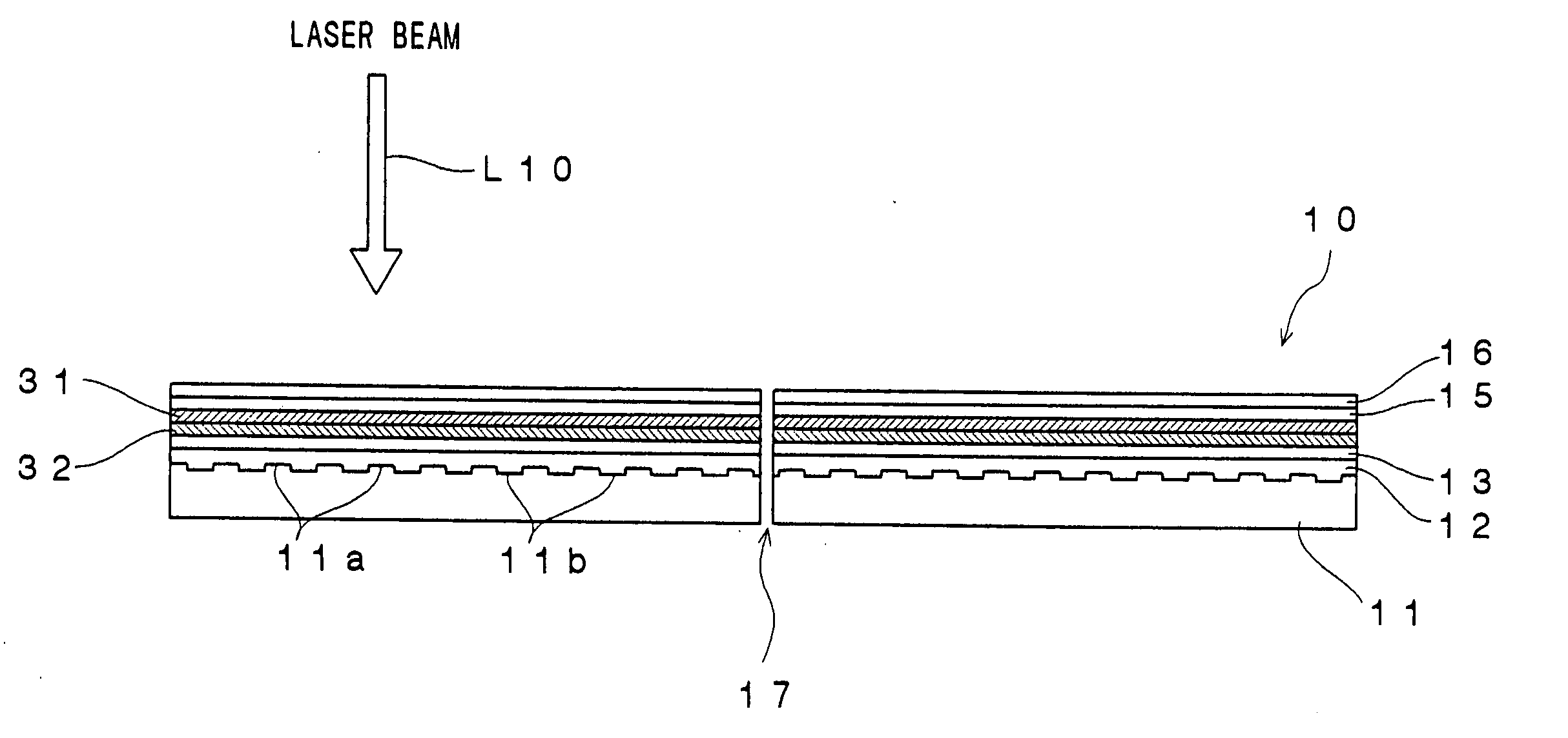
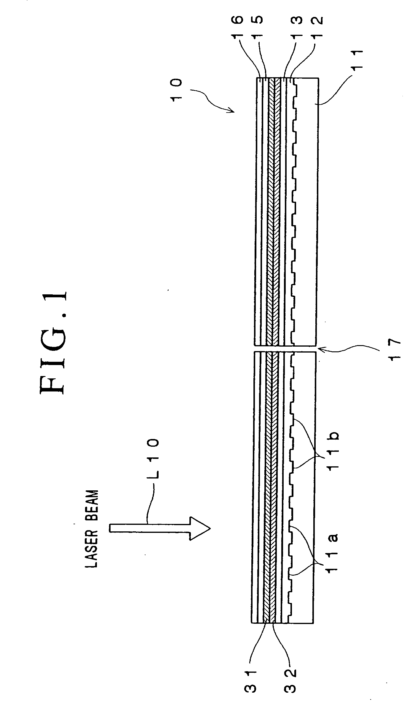
[0136] An optical recording medium sample # 1 having the same structure as that shown in FIG. 1 was fabricated in the following manner.
[0137] A polycarbonate substrate having a thickness of 1.1 mm and a diameter of 120 mm was first set on a sputtering apparatus. Then, a reflective layer containing Ag as a primary component and having a thickness of 100 nm, a second dielectric layer containing a mixture of ZnS and SiO2 and having a thickness of 28 nm, a second recording layer containing Cu as a primary component, added with 21 atomic % of Mg and having a thickness of 5 nm, a first recording layer containing Si as a primary component and having a thickness of 5 nm and a first dielectric layer containing the mixture of ZnS and SiO2 and having a thickness of 22 nm were sequentially formed on the polycarbonate substrate using the sputtering process.
[0138] The mole ratio of ZnS to SiO2 in the mixture of ZnS and SiO2 contained in the first dielectric layer and the second dielectric layer...
working example 2
[0156] An optical recording medium sample # 3 was fabricated in the manner of the optical recording medium sample # 1, except that a second recording layer containing Al as the primary component and added with 17 atomic % of Mg was formed.
[0157] Similarly to the Working Example 1, data were recorded in the optical recording medium sample # 3, and the first recording layer, the second recording layer, the first dielectric layer and the second dielectric layer in the optical recording medium sample # 3 were observed.
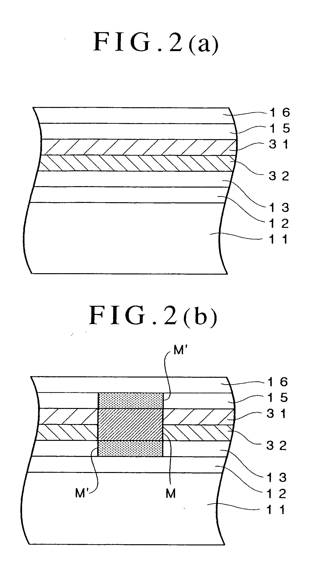
[0158] It was observed in the optical recording medium sample # 3 that materials of the first recording layer and the second recording layer were mixed at a region where the record mark was formed and that materials of the first recording layer and the second recording layer were not mixed in the blank region.
[0159] Further, ZnS crystal was observed at regions of the first dielectric layer and the second dielectric layer adjacent to the record mark in the optical record...
working example 3
[0161] An optical recording medium sample # 4 was fabricated in the manner of the optical recording medium sample # 1, except that a second recording layer containing Cu as the primary component and added with 23 atomic % of Al and 12.8 atomic % of Au was formed.
[0162] Data were recorded in the optical recording medium sample # 4 using the optical recording medium evaluation apparatus used in the Working Example 1 and using a laser beam whose power was modulated in accordance with the single pulse pattern shown in FIG. 3.
[0163] The ground power Pb1 of the single pulse pattern was set to 0.1 mW and the recording power Pw1 thereof was set to 3.8 mW.
[0164] The other recording conditions were the same as those used in the Working Example 1.
[0165] Similarly, data were recorded in the optical recording medium sample # 4 by modulating the power of the laser beam in accordance with the basic pulse train pattern shown in FIG. 4.
[0166] The width of each pulse of the basic pulse train pat...
PUM
| Property | Measurement | Unit |
|---|---|---|
| power | aaaaa | aaaaa |
| total thickness | aaaaa | aaaaa |
| thickness | aaaaa | aaaaa |
Abstract
Description
Claims
Application Information
 - R&D
- Intellectual Property
- Life Sciences
- Materials
- Tech Scout
- Unparalleled Data Quality
- Higher Quality Content
- 60% Fewer Hallucinations
Browse by: Latest US Patents, China's latest patents, Technical Efficacy Thesaurus, Application Domain, Technology Topic, Popular Technical Reports.
© 2025 PatSnap. All rights reserved.Legal|Privacy policy|Modern Slavery Act Transparency Statement|Sitemap|About US| Contact US: help@patsnap.com