Semiconductor device and method for forming the same

a technology of semiconductors and devices, applied in the direction of semiconductor devices, basic electric elements, electrical equipment, etc., can solve the problems of increasing leakage current, reducing device yield, and difficulty in engineering the magnitude of compressive stress applied to the channel region, so as to improve the operation speed

Inactive Publication Date: 2006-04-20
SAMSUNG ELECTRONICS CO LTD
View PDF4 Cites 29 Cited by
  • Summary
  • Abstract
  • Description
  • Claims
  • Application Information

AI Technical Summary

Benefits of technology

[0015] It is therefore a feature of the present invention to provide a semiconductor device capable of improving an operation speed without regard to a design rule and a method for forming the same.

Problems solved by technology

However, this method requires various processes such as forming a strained silicon-germanium layer, relaxing the strained silicon-germanium layer, and forming a silicon layer, so that device yield is reduced.
It is difficult to engineer the magnitude of the compressive stress applied to the channel region.
With high integration of semiconductor devices in condsideration of high-performance, high-speed, economics, there are several problems such as a short channel effect like punch-through characteristic as a channel length of a conventional planar MOSFET becomes short, the increment of a parasitic capacitance (a junction capacitance) between a junction region and a substrate, the increment of leakage current.
This technique will be described referring to FIG. 3 because it is unsuitable to apply the method of FIG. 1 to the MOSFET using the SOI substrate.

Method used


Image

  • Semiconductor device and method for forming the same
  • Semiconductor device and method for forming the same
  • Semiconductor device and method for forming the same

Examples


Embodiment Construction

[0046] In the specification, the thickness of layers and regions are exaggerated for clarity. It will be understood that when an element such as a layer, region or substrate is referred to as being “on” or “onto” another element, it can be directly on the other element or intervening elements may also be present. It will also be understood that, although the terms first, second, etc. may be used herein to describe various elements, these elements should not be limited by theses terms. These terms are only used to distinguish one element from another. For example, a first element could be termed a second element, and similarly, a second element could be termed a first element, without departing from the scope of the present invention.

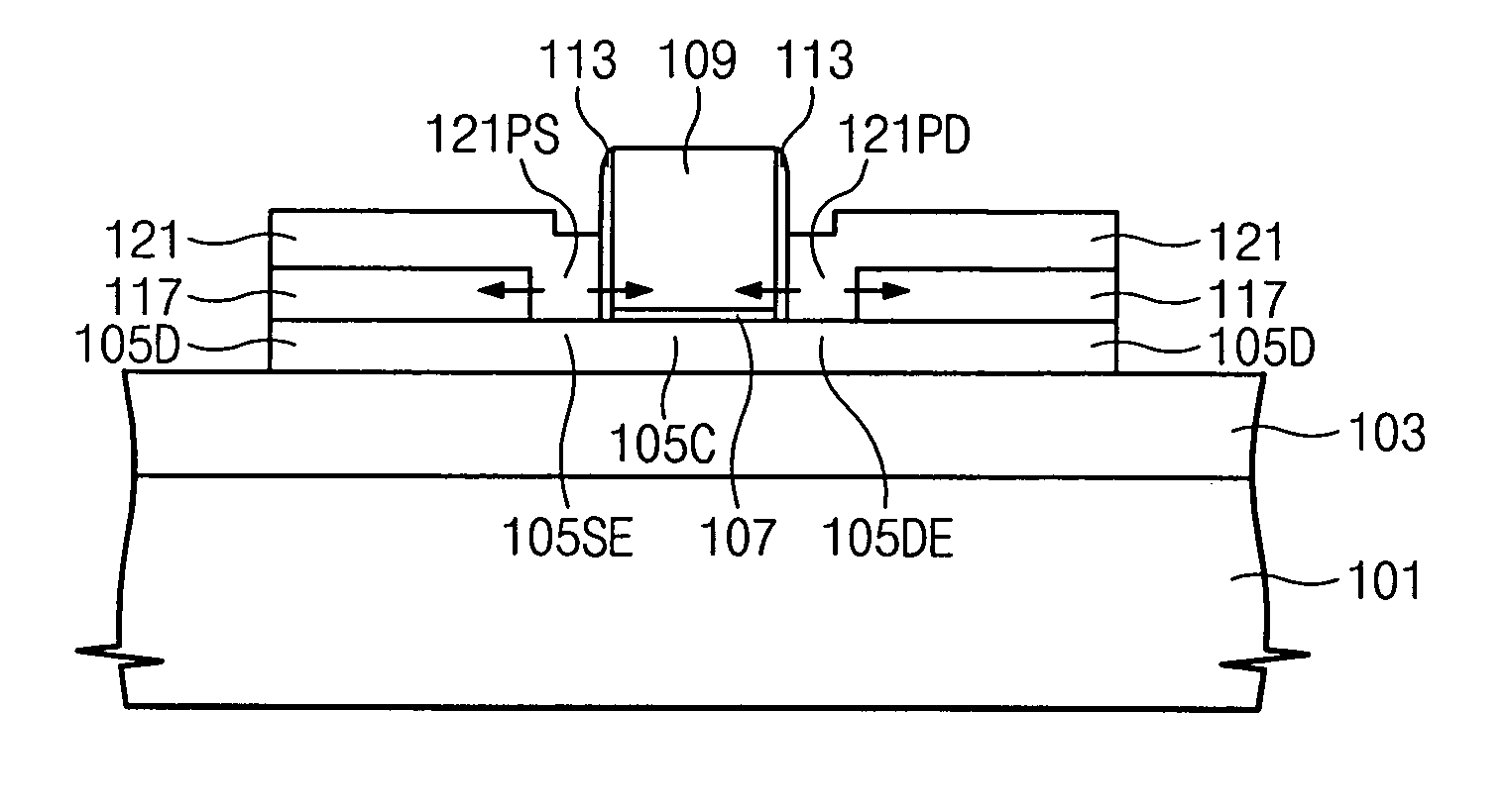
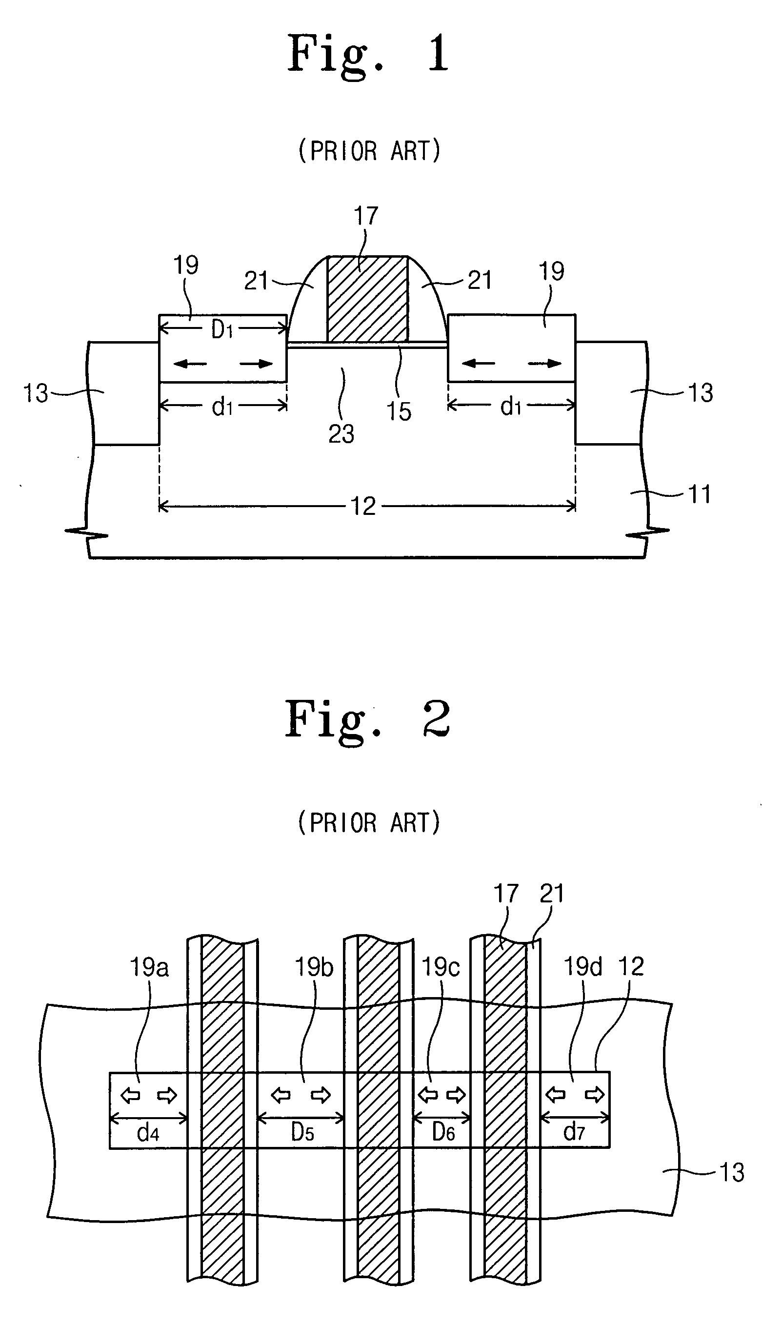
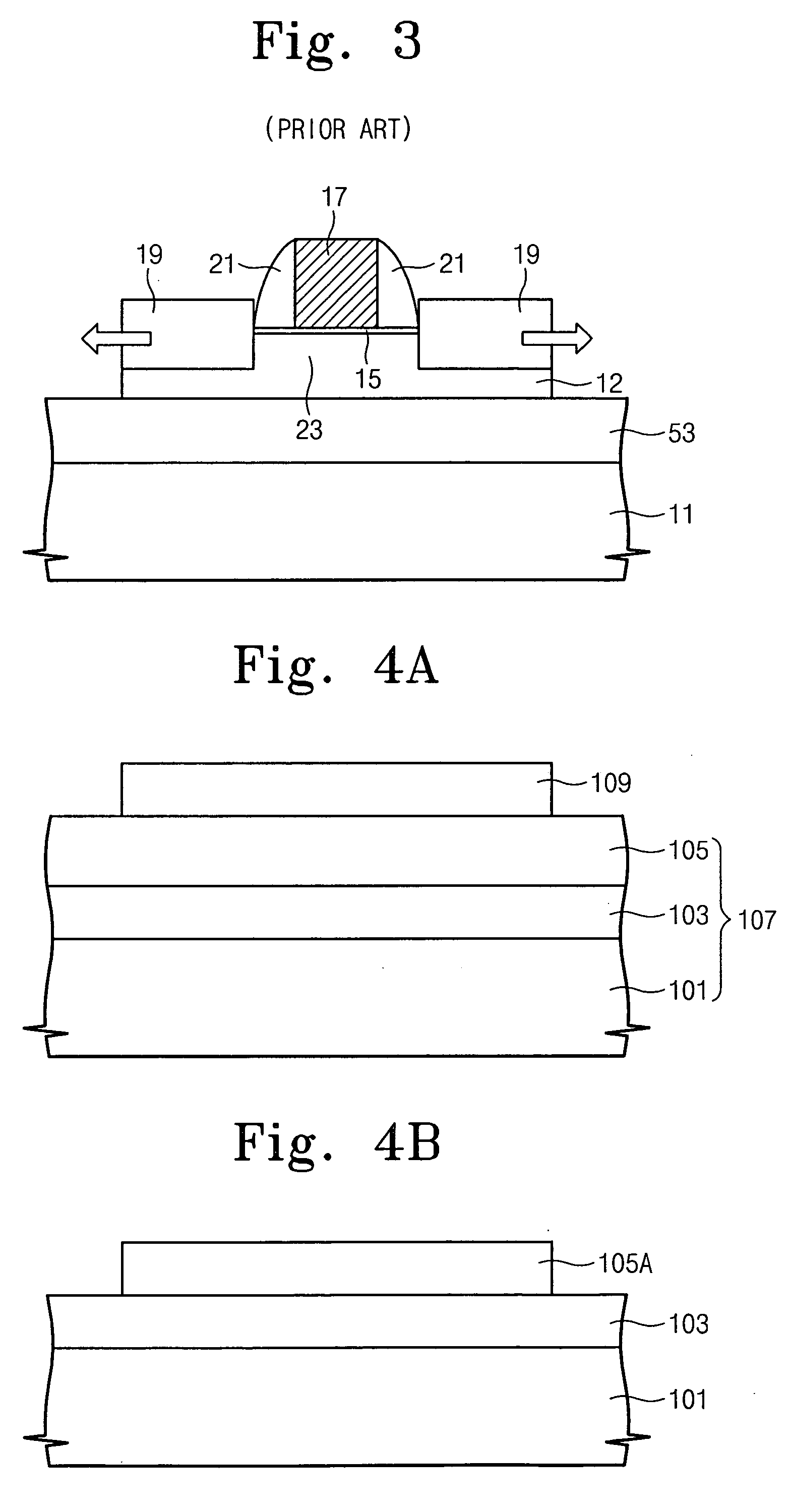
[0047] The present invention relates to a method for forming a semiconductor device, and more specifically, to a MOSFET and a method for forming a MOSFET. Hereinafter, a P-type MOSFET and a method for forming the same will be described by way of example...


PUM


Abstract

The present invention disclosed herein is a semiconductor device and a method for forming the same. The semiconductor device includes a first semiconductor pattern defining an active region, second semiconductor patterns placed on the first semiconductor pattern apart from each other, an insulated gate electrode spaced apart from the second semiconductor patterns to be placed therebetween, and stress generating patterns filling intervals between the insulated gate electrode and the second semiconductor patterns. The stress generating patterns apply a stress to a channel region defined by the first semiconductor pattern under the gate electrode, thereby increasing carrier mobility.

Description

CLAIM OFF PRIORITY [0001] The present application claims priority from Korean Patent Application No. 10-2004-0084055 filed on Oct. 20, 2004, the contents of which are hereby incorporated by reference herein in their entirety. FIELD OF THE INVENTION [0002] The present invention is directed generally to semiconductor devices and a method for forming the same, and more particularly to a MOS Field Effect Transistor and a method for forming the same. BACKGROUND OF THE INVENTION [0003] The MOSFET is an important device in semiconductor integrated circuits. The MOSFET includes source / drain regions formed on a substrate, and a gate electrode on a channel defined therebetween. The gate electrode is insulated from the channel by a gate insulating layer. An electric field is created by applying proper bias voltage to the gate electrode while the MOSFET is operated. The electric field is used to control formation of a channel under the gate electrode. In addition, proper bias voltage is applied...

Claims


Application Information

Patent Timeline
Patent Type & Authority Applications(United States)
IPC IPC(8): H01L29/76
CPCH01L21/823807H01L21/823864H01L21/84H01L27/1203H01L29/66628H01L29/66636H01L29/7834H01L29/7842H01L29/7843H01L29/785H01L21/18
Inventor MAEDA, SHIGENOBU
Owner SAMSUNG ELECTRONICS CO LTD
Why Eureka
Try Eureka