Integrated circuit optical detector for biological detection

an integrated circuit and optical detector technology, applied in the field of optical detectors, can solve the problems of unreliable testing results, difficult to process conduction data using noise reduction techniques, and relatively expensive process, and achieve the effect of high sensitivity

Inactive Publication Date: 2006-04-20
THE HONG KONG UNIV OF SCI & TECH
View PDF17 Cites 42 Cited by
  • Summary
  • Abstract
  • Description
  • Claims
  • Application Information

AI Technical Summary

Benefits of technology

[0007] One of the major advantages of the present invention is that the IC optical detector and the method are fully CMOS compatible. Another advantage is that the detecting method is completely automated and so that the result is directly read out without external optical scanner needed Still another advantage is that the IC optical detector and the method provide a high sensitivity for low concentration detection compared with most existing systems. Still another advantage is that the IC optical detector and the method are capable of working with ordinary light sources instead of expensive and highly specific UV light sources.

Problems solved by technology

Thus, the process is relatively expensive and inconvenient.
Further, such conventional method requires specific color filters that are composed of very complicated film structure.
Finally, the fluorescence and radioactive signal intensity degrade with time and can cause large variations in the sampled data, such that the testing result might be unreliable.
Also it is difficult to process the conduction data using noise reduction techniques.

Method used


Image

  • Integrated circuit optical detector for biological detection
  • Integrated circuit optical detector for biological detection
  • Integrated circuit optical detector for biological detection

Examples


embodiment

Preferred Embodiment

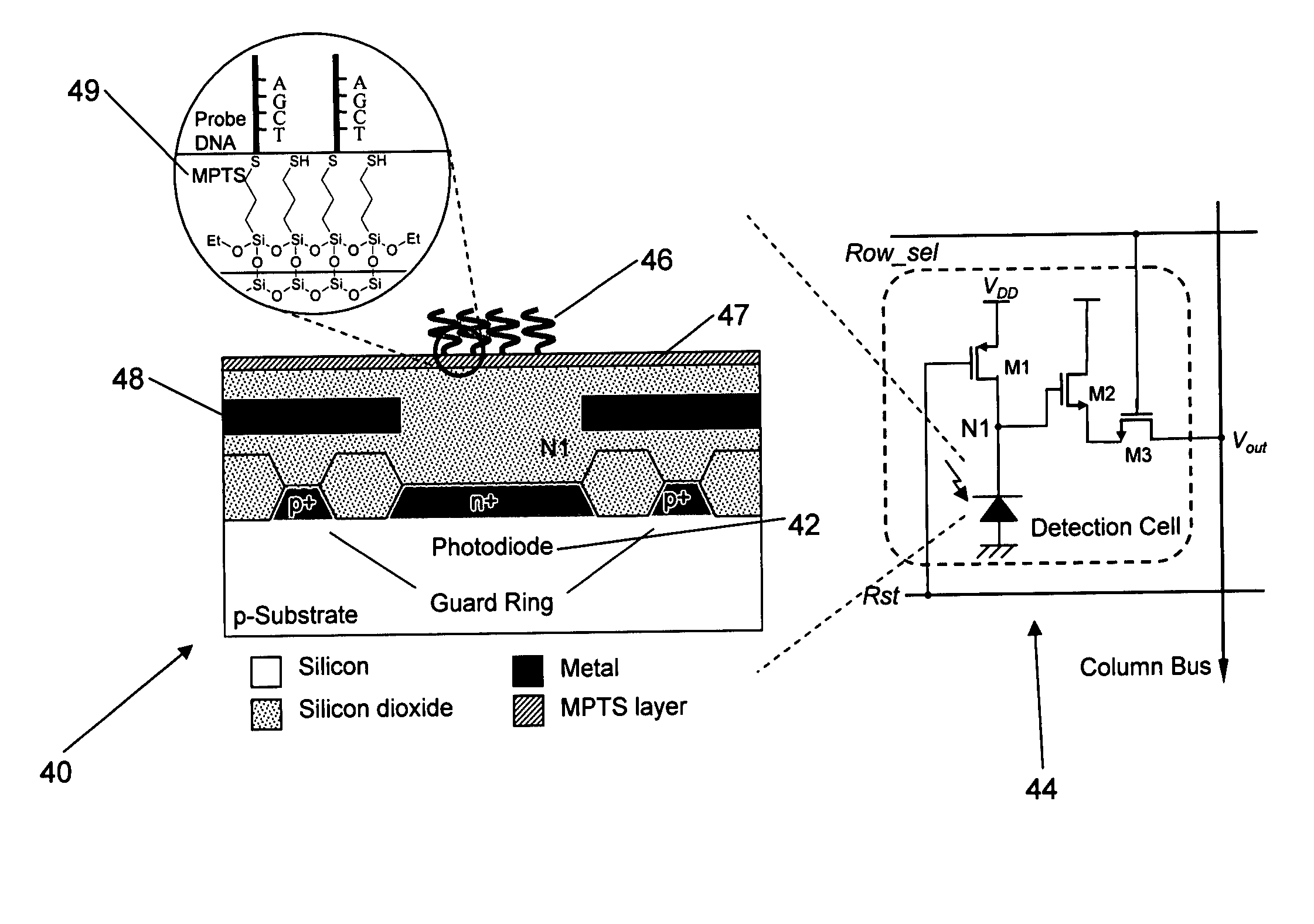
[0035]FIG. 8 shows a preferred embodiment of the present invention, that of detection and identification of DNA sequences in a sample. The DNA fragment detection process using the IC optical detector is as described in previous Figures. Typically, the IC optical detector includes a substrate (not shown in FIG. 8) and an IC including at least one photodiode array 80. The photodiode array 80 can be CMOS image sensors or charge-coupled device (CCD) array. The surface 82 of the photodiode array 80 usually has a plurality of test sites and is modified in order to form covalent bonding with the a plurality of DNA probes 84 adapted for receiving at least one test sample. In one embodiment, the photodiode array 80 is formed within the substrate such that the surface 82 is the substrate surface.

[0036] Typically, a specific sample DNA 88 is modified with Adenosine polymer (poly A) tails. These sample DNA 88 may be applied to the photodiode array surface 82 in solution for...


PUM

PropertyMeasurementUnit
diameteraaaaaaaaaa
optical signalsaaaaaaaaaa
electricalaaaaaaaaaa

Abstract

This invention provides an integrated circuit (IC) optical detector. The IC optical detector comprises a substrate and an IC. The substrate comprises a plurality of test sites defined thereon. The test sites comprise a surface suitably treated for coating of at least one test sample. The at least one test sample is capable of being changed by a reaction. The IC comprises at least one optical sensor array for simultaneously receiving and sensing optical signals from the test sites during operations Presence of at least one changed test sample at a test site changes the quantity of light directed through the test site. The change in quantity of light is detectable by the sensor array. The optical sensor array further converts the sensed optical signals to electrical signals. The IC automatically processes and outputs the electrical signals during operation. This invention further provides a method for detecting a specific sample within at least one test sample. The method comprises securing said test sample on a plurality of test sites defined on a substrate; processing said test sample to allow said test sample to be optically differentiated; directing a light at said test sample; simultaneously receiving and sensing optical signals from said test sample using at least one optical sensor array of an IC; converting said sensed optical signals to electrical signals by said optical sensor array; and automatically processing and outputting said electrical signals by said IC to detect said specific sample within said test sample.

Description

FIELD OF INVENTION [0001] The present invention is related to an optical detector, and particularly to an integrated circuit (IC) optical detector used for biological sample detection. BACKGROUND OF INVENTION [0002] The introduction of high-density DNA micro-arrays has significantly reduced the time and cost for DNA detection through miniaturization and automation that are made available by some advanced IC fabrication technologies. The dominant DNA micro-array based detection systems rely on fluorescence or radioactive methods to discriminate matched (ie hybridized) and unmatched (unhybridized) DNA samples for a given testing probe. Referring to FIG. 1, conventionally, a solid support (eg a DNA array chip) 10 with DNA probes 12 is provided as shown in FIG. 1(a). It is to be noted that this DNA “chip” is not related to a packaged integrated circuit device which is also called a “chip”. The sample DNA fragments 14 typically have one or more fluorescent labels. The sample DNA fragment...

Claims


Application Information

Patent Timeline
Patent Type & Authority Applications(United States)
IPC IPC(8): C12Q1/68C12M1/34
CPCB01L3/5088C12Q1/6825G01N21/6428G01N21/6454
Inventor CHAN, MANSUNLI, JIONGWANG, YIJINLU, ZUHONG
Owner THE HONG KONG UNIV OF SCI & TECH
Why Eureka
Try Eureka