Semiconductor device and manufacturing method thereof
a semiconductor and manufacturing method technology, applied in non-linear optics, instruments, optics, etc., can solve problems such as complicated manufacturing of tft, and achieve the effects of improving productivity and yield, and reducing the number of photomasks
- Summary
- Abstract
- Description
- Claims
- Application Information
AI Technical Summary
Benefits of technology
Problems solved by technology
Method used
Image

Examples
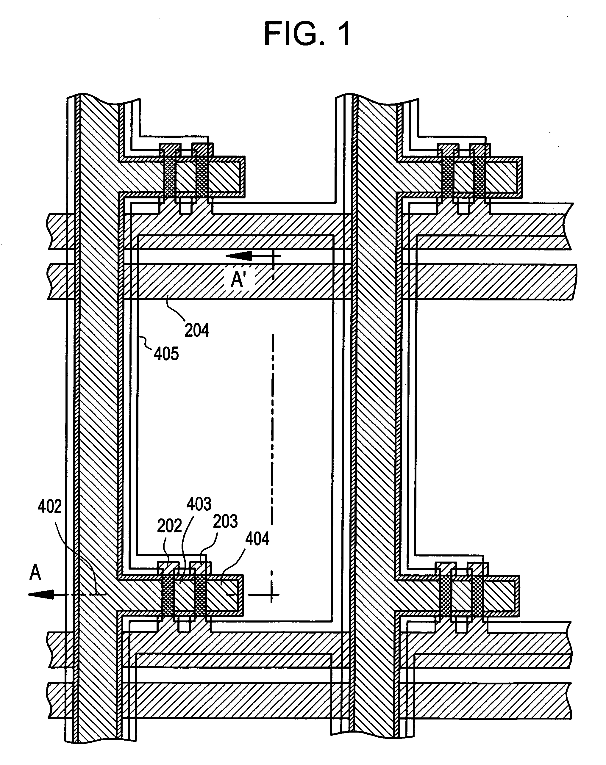
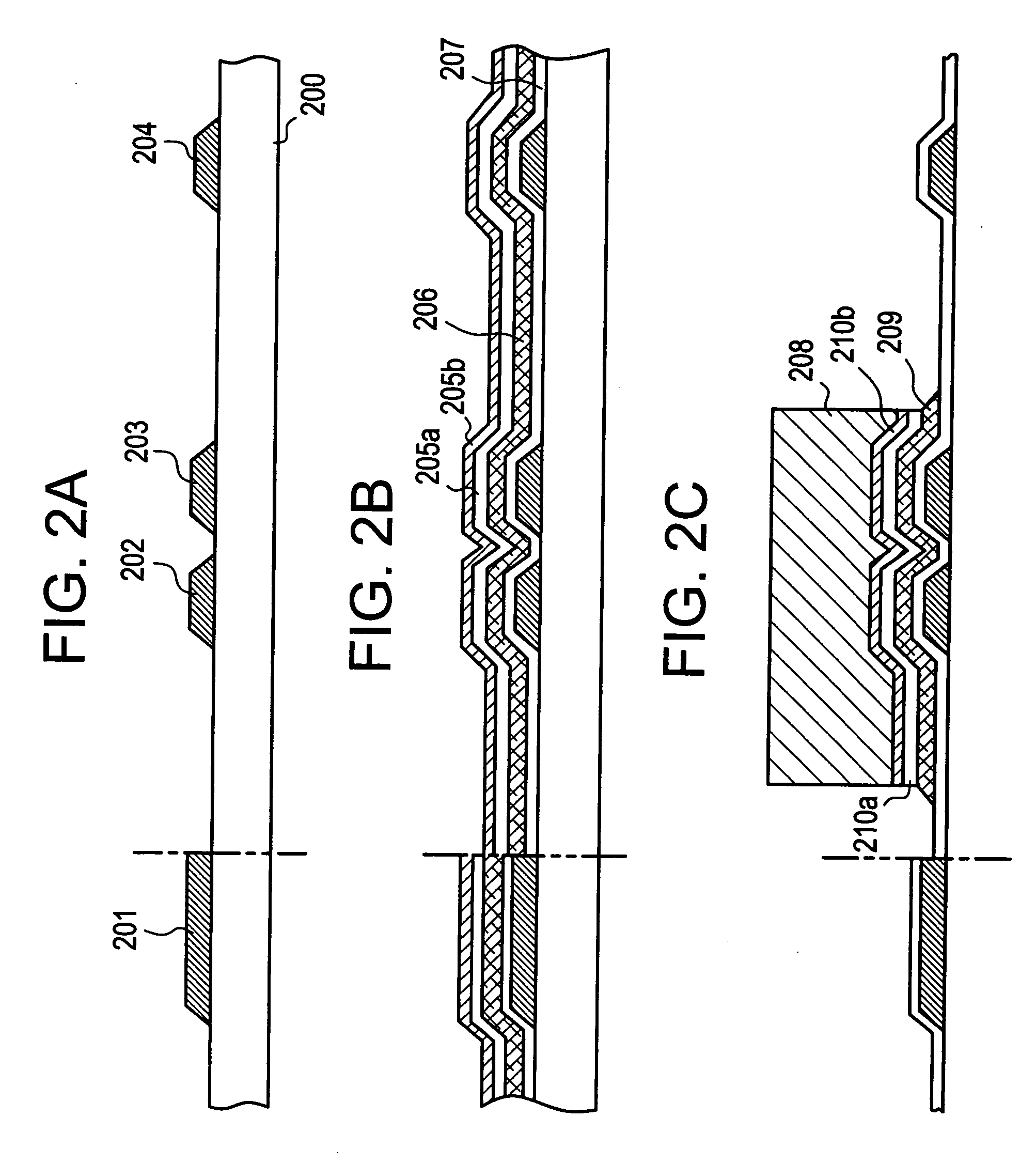
embodiment mode 1
[0099] First, a conductive film is formed on the entire surface of a substrate. The conductive film is formed into a desired shape through a first photolithography step. As a material of the conductive film, an element selected from W, WSix, Al, Ti, Mo, Cu, Ta, Cr, Ni, and Mo, a film containing as a main component an alloy material or compound material containing the element as a main component, or a multi-layer film thereof can be enumerated. Later, the conductive film is etched to become a gate electrode or a gate wiring or a retention capacitance wiring.
[0100] Next, an insulating film is formed on the entire surface of the conductive film. Later, the insulating film functions as a gate insulating film. A first amorphous semiconductor film and a second amorphous semiconductor film containing an impurity element with one conductivity type (n-type or p-type) and a conductive film comprising a metallic material (a metallic material containing Al, Ti, Mo, Cu, Ta, Cr, Ni or Mo as a ma...
embodiment mode 2
[0108] First, a conductive film is formed on the entire surface of a substrate. The conductive film is formed into a desired shape through a first photolithography step. Later, the conducive film is etched to form a gate electrode or a gate wiring or a storage capacitance wiring.
[0109] Next, an insulating film is formed on the entire surface of the conductive film. Later, the insulating film functions as a gate insulating film. A first amorphous semiconductor film and a second amorphous semiconductor film containing an impurity element with one conductivity type (n-type or p-type) and a conductive film comprising metallic material (metallic material containing Al, Ti, Mo, Cu, Ta, Cr, Ni or Mo as a main component) are deposited on the insulating film.
[0110] Then, an unnecessary portion of the layered film formed of the first amorphous semiconductor film and the second amorphous semiconductor film containing an impurity element with one conductivity type (n-type or p-type) and the c...
embodiment 2
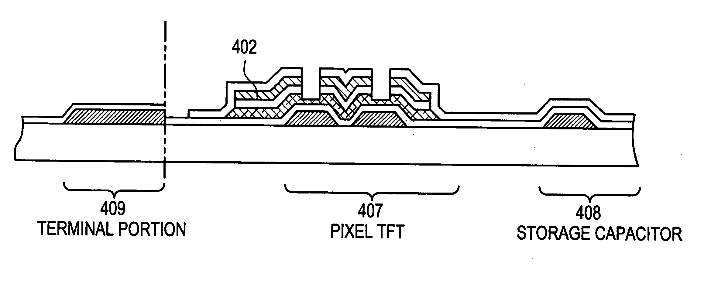
[0135] The semiconductor display device including the channel etch type TFT in the pixel portion has been described in Embodiment 1, while a semiconductor display device including a channel stop type TFT in the pixel portion will be described in Embodiment 2 with reference to FIGS. 5A to 7C.
[0136] First, a semiconductor display device is manufactured by using a substrate 500 with light transmittance. As the substrate 500, a glass substrate such as barium borosilicate glass and alumino borosilicate glass, as represented by #7059 glass and #1737 glass manufactured by Corning Inc., can be used. Besides, a light transmitting substrate such as a quartz substrate and a plastic substrate can also be used as the substrate 500.
[0137] After forming a conductive film on the entire surface of the substrate 500, a first photolithography step is conducted to form a resist mask. An unnecessary portion is removed by etching to form gate electrodes 502 and 503, a storage capacitor wiring 504, and ...
PUM
| Property | Measurement | Unit |
|---|---|---|
| angle | aaaaa | aaaaa |
| temperature | aaaaa | aaaaa |
| taper angle | aaaaa | aaaaa |
Abstract
Description
Claims
Application Information
 - R&D
- Intellectual Property
- Life Sciences
- Materials
- Tech Scout
- Unparalleled Data Quality
- Higher Quality Content
- 60% Fewer Hallucinations
Browse by: Latest US Patents, China's latest patents, Technical Efficacy Thesaurus, Application Domain, Technology Topic, Popular Technical Reports.
© 2025 PatSnap. All rights reserved.Legal|Privacy policy|Modern Slavery Act Transparency Statement|Sitemap|About US| Contact US: help@patsnap.com