Refresh control method of a semiconductor memory device and semiconductor memory device

a semiconductor memory and control method technology, applied in the field of refresh control, can solve the problems of not being able to achieve sufficient current reducing effect as a whole, the limit of current consumption reduction of the dram, and the inability to reduce the current consumption of the semiconductor memory device at the time of self-refresh, so as to achieve the effect of reducing the size of the holding area itself, and increasing the accumulated charg

Inactive Publication Date: 2006-04-27
PS4 LUXCO SARL
View PDF0 Cites 112 Cited by
  • Summary
  • Abstract
  • Description
  • Claims
  • Application Information

AI Technical Summary

Benefits of technology

[0039] As described above, according to the present invention, the subject of the self-refresh is limited to the data holding area which is set in a portion of the memory array, data is copied from the data holding area to a portion of the copy area or the plurality of memory cells on the same bit line or the same pair of bit lines, and a word line from which data is copied and a word line to which the data is copied are selected and driven at the same time when the self-refresh is executed. Therefore, longer period refresh can be realized, and the current consumption of the semiconductor memory device at the time of self-refresh can largely be reduced. Tha

Problems solved by technology

However, when it is desired to increase the battery using time of the mobile device, the current consumption can not be reduced sufficiently even if the conventional partial array self-refresh method is employed.
However, in terms of the ease-of-use of the mobile device, it is necessary to secure the data-holding capacity to a

Method used


Image

  • Refresh control method of a semiconductor memory device and semiconductor memory device
  • Refresh control method of a semiconductor memory device and semiconductor memory device
  • Refresh control method of a semiconductor memory device and semiconductor memory device

Examples


first embodiment

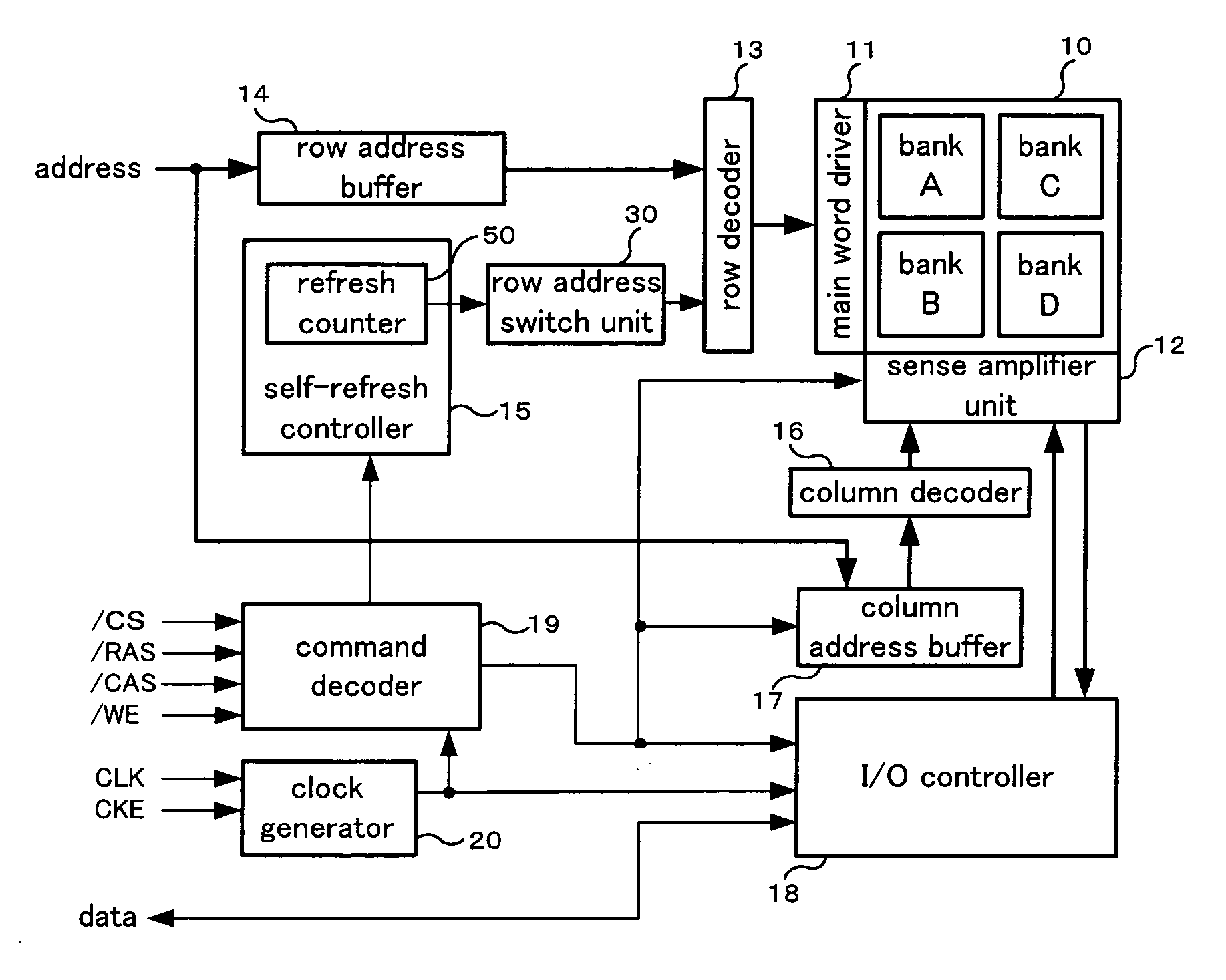
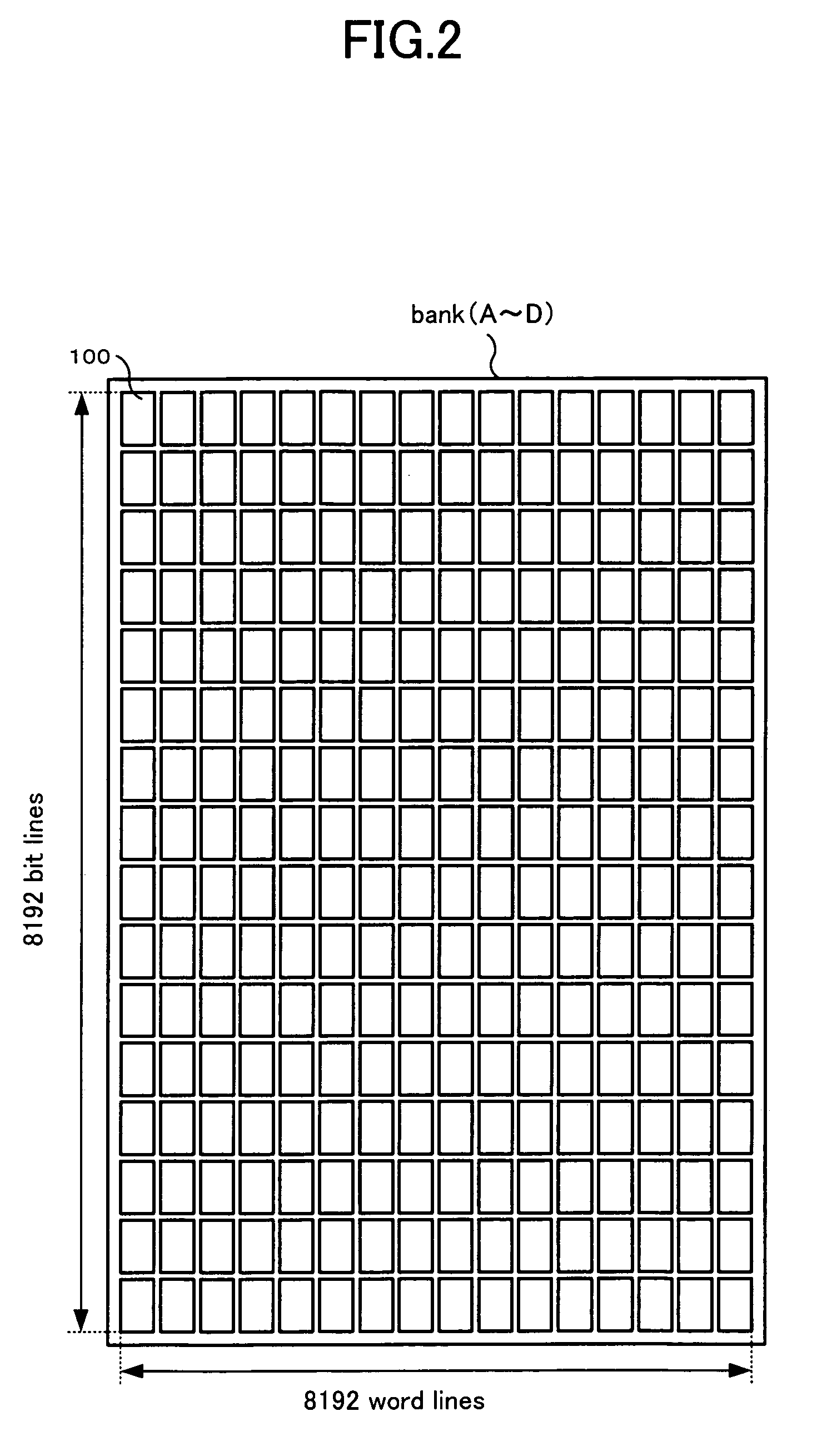
[0076]FIG. 1 is a block diagram showing the entire configuration of a DRAM of a first embodiment. In this example, the DRAM has storage capacity of 256 Mbits, and four banks. The DRAM shown in FIG. 1 has a memory array 10 in which a large number of memory cells are arranged in a matrix form in a direction of rows and in a direction of columns. Each memory cell stores 1 bit. The memory array 10 is divided into four banks which are 64 Mbits storage regions (these banks are shown as banks A, B, C and D in the drawing). These banks have the same configuration. Each bank is designated based on a bank selection signal of 2 bits coming with an address signal.

[0077] Provided around the memory array 10 are a main word driver 11, a sense amplifier unit 12, a row decoder 13, a row address buffer 14, a self-refresh controller 15, a column decoder 16, a column address buffer 17, an I / O controller 18, a command decoder 19 and a clock generator 20. Further, a row address switch unit 30 for realiz...

second embodiment

[0154] Next, FIG. 22 is a block diagram showing the entire configuration of a DRAM of a second embodiment which controls the switching operation of the supply voltage in the self-refresh. The entire circuit of the DRAM of the second embodiment is roughly divided into two portions, i.e., an array circuit C1 and a peripheral circuit C2. Basic configurations of the array circuit C1 and the peripheral circuit C2 are common to the DRAM of the first embodiment. In FIG. 22, constituent elements which are common to FIG. 1 are designated with the same numbers.

[0155] In the DRAM of the second embodiment, in addition to the above facts, a power supply unit 60 which generates a supply voltage required for operations of the array circuit C1 and the peripheral circuit C2 and supplies the same to various portions is provided. The power supply unit 60 includes an array power supply 61 which generates supply voltages (array voltages) to be supplied to the array circuit C1, and a peripheral power su...


PUM


Abstract

A refresh control method of a semiconductor memory device which controls a self-refresh operation to hold data in a memory array having a plurality of memory cells disposed at intersections of word lines corresponding to row addresses and bit lines corresponding to column addresses, comprising: a step for dividing the memory array into a holding area used as a copy source which includes memory cells on a predetermined number of word lines, and a copy area used as a copy destination which includes memory cells on word lines to which entire data of the holding area is to be copied, a step for executing copy operation in which data of each memory cell of the holding area is copied to one or more memory cells in the copy area on the same bit line or the same pair of bit lines before executing the self-refresh operation, and a step for executing the self-refresh operation in which a row address of the holding area is designated and a corresponding word line is selected and driven, and at the same time, one or more word lines in the copy area corresponding to the selected word line are selected and driven.

Description

BACKGROUND OF THE INVENTION [0001] 1. Field of the Invention [0002] The present invention relates to a field of refresh technique for a pseudo SRAM or a DRAM (Dynamic Random Access Memory) mounted on a mobile device, and more particularly, to a partial array self-refresh type technical field only for a partial area which is set in a memory array in long period refresh operation for reducing power consumption as compared with normal state. [0003] 2. Related Art [0004] In recent years, a large-capacity DRAM is mounted in a mobile device such as a cellular phone in general. To reduce the power consumption when the mobile device is in a standby mode, it is strongly desired to reduce the consumption current in a data holding state of the DRAM. To that end, there has been developed a DRAM having long period refresh function for executing self-refresh operation for sufficiently long period as compared with normal operation. [0005] In long period refresh, as an effective technique for furth...

Claims


Application Information

Patent Timeline
IPC IPC(8): G11C7/00
CPCG11C11/406G11C11/40615G11C11/40618G11C11/40622
Inventor RIHO, YOSHIROKAJIGAYA, KAZUHIKO
Owner PS4 LUXCO SARL
Why Eureka
Try Eureka