Method for fabricating connection terminal of circuit board

Active Publication Date: 2006-05-04
PHOENIX PRECISION TECH CORP
View PDF4 Cites 12 Cited by
  • Summary
  • Abstract
  • Description
  • Claims
  • Application Information

AI Technical Summary

Benefits of technology

[0015] A further objective of the present invention is to provide a method for fabricating connection terminals of the circuit board so as to prevent problems such as reduced yield, and increased fabrication complexity and cost caused by multiple deposition and removal of the resist and conductive layer in the conventional electroplating process for forming

Problems solved by technology

These dynamic changes have brought in many challenges for package technology of the semiconductor chip.
So, the production cost is increased due to difficulty in the template development.
It is also difficult for the soldering material to pass through the minimized openings of the template, creating bottleneck in terms of the process.
As a result, the amount and shape of the solder material used in the next printing will not match those according to the designed specification.
In the actual operation, the template would have to be wiped clean after being applied to printing for certain number of times. Otherwise, it is very likely to create mismatched shape and size of the soldering material, causing process inconvenien

Method used


Image

  • Method for fabricating connection terminal of circuit board
  • Method for fabricating connection terminal of circuit board
  • Method for fabricating connection terminal of circuit board

Examples


Example

[0025] The present invention is described in the following with specific embodiments, so that one skilled in the pertinent art can easily understand other advantages and effects of the present invention from the disclosure of the invention. The present invention may also be implemented and applied according to other embodiments, and the details may be modified based on different views and applications without departing from the spirit of the invention.

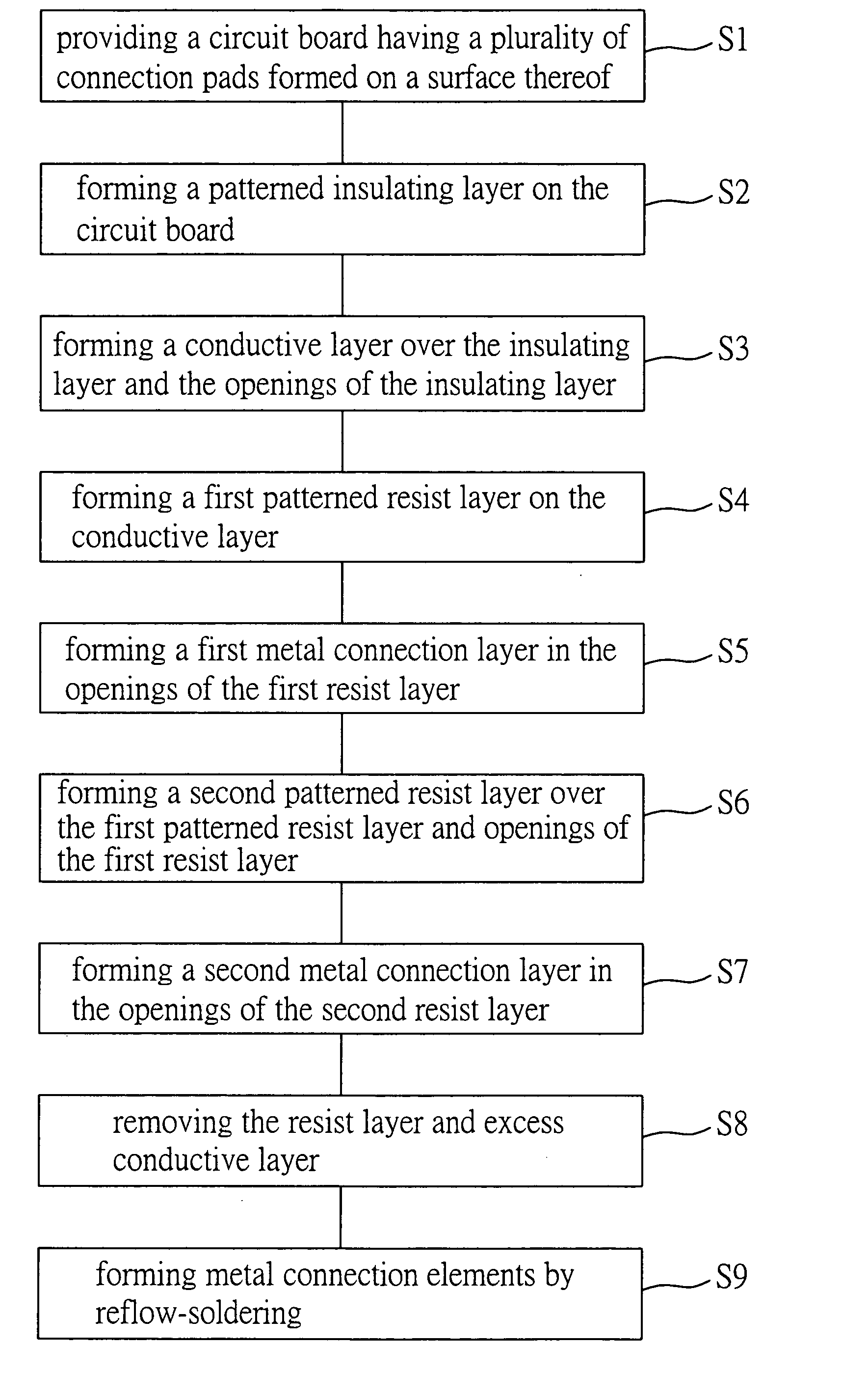
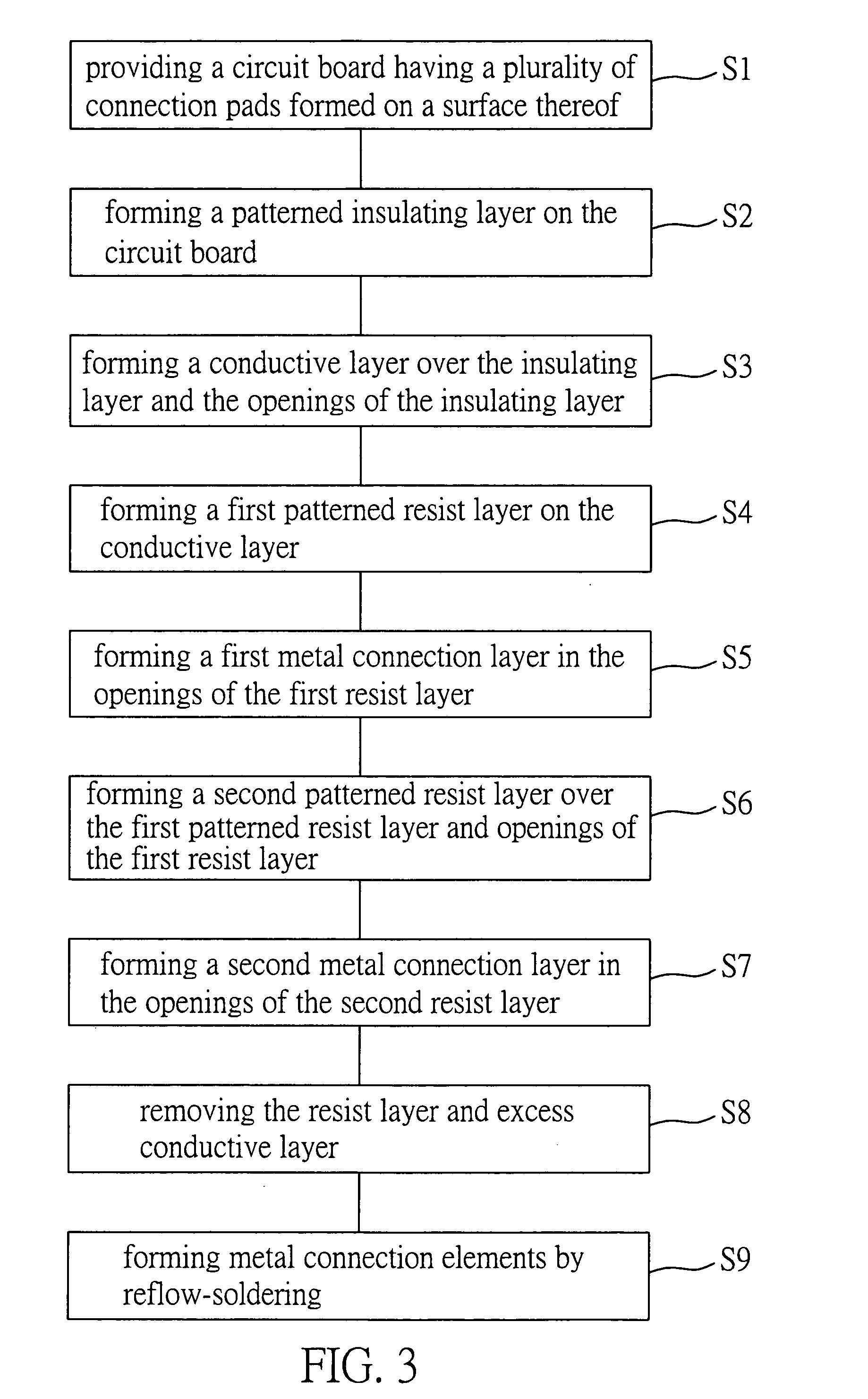
[0026] Referring to FIG. 3 for illustrating a method of fabricating the connection terminals of the circuit board according to the present invention, and in accompany with the cross-sectional views of the fabrication process illustrated in FIGS. 4A through to 4I, so as to describes the embodiments of the invention.

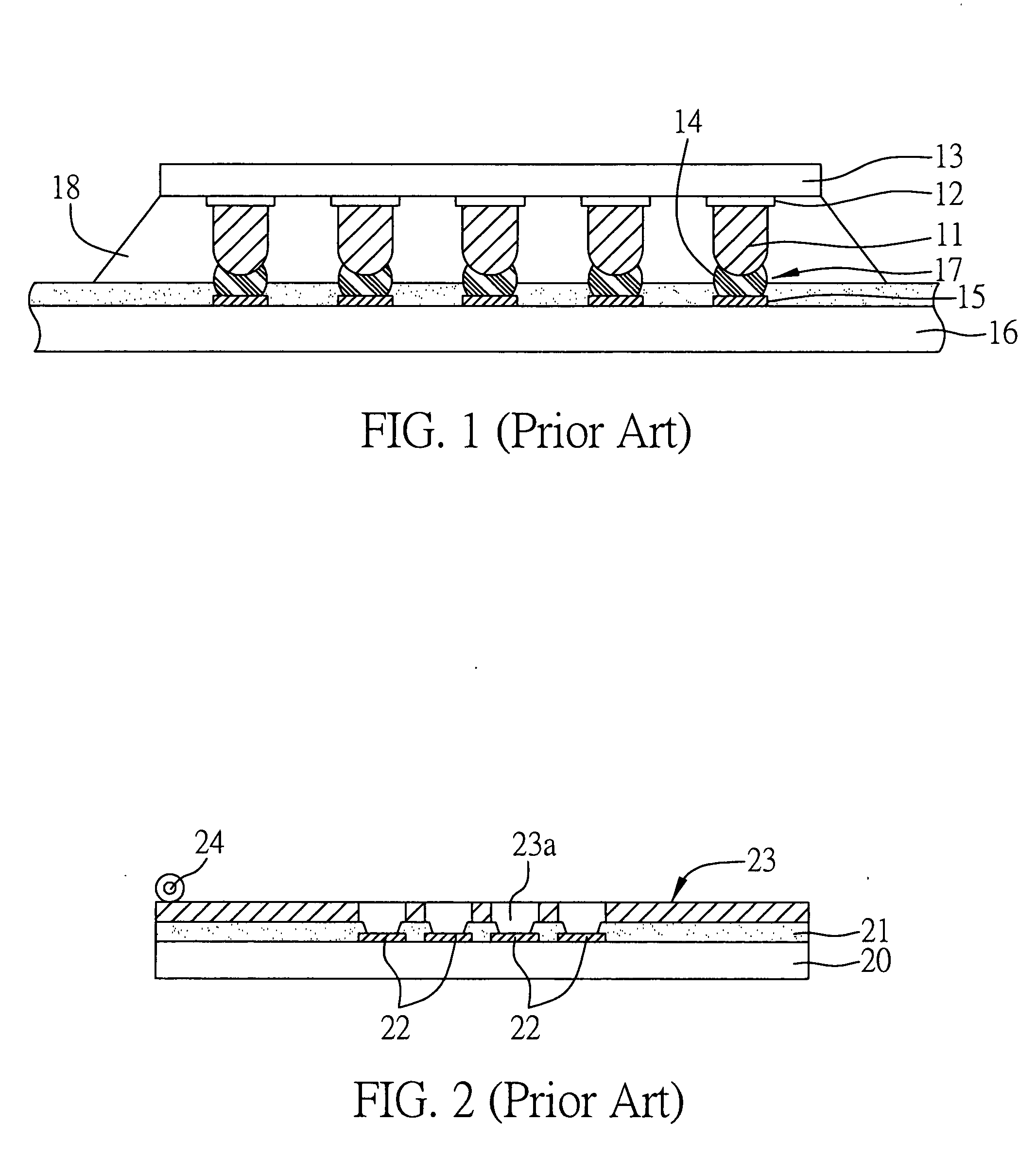
[0027] In step S1, a circuit board 401 having a plurality of connection pads 403 formed thereon (shown in FIG. 4A) is provided. The connection pads 403 may be metal connection pads for connecting to the metal bumps of the f...


PUM

PropertyMeasurementUnit
Sizeaaaaaaaaaa
Electrical conductoraaaaaaaaaa
Heightaaaaaaaaaa

Abstract

A method for fabricating connection terminals of a circuit board is proposed. The method involves providing a circuit board with connection pads thereon, forming an insulating layer with first openings over the circuit board to expose the connection pads, forming a conductive layer over the insulating layer, forming a first resist layer with second openings over the conductive layer to partially expose the conductive layer, electroplating a first metal connection layer on the exposed conductive layer, followed by forming a second resist layer with third openings over the first conductive layer to partially expose the first metal connection layer, and electroplating a second metal connection layer on the exposed first connection layer, and removing portions of the first and second resist layers and conductive layer covered by the first and second resist layers to form metal connection material of different heights and sizes on the connection pads.

Description

BACKGROUND OF THE INVENTION [0001] 1. Field of the Invention [0002] The invention relates to a method for fabricating connection terminals of a circuit board, and more particularly, to a method for fabricating metal connection materials of different heights and sizes simultaneously on connection pads of the circuit board. [0003] 2. Description of the Related Art [0004] In the recent years, electrical products such as notebook (NB) computer, mobile phone, personal digital assistant (PDA), and digital camera are developed in a more and more compact size while their operation speeds are getting faster by demands. These dynamic changes have brought in many challenges for package technology of the semiconductor chip. As the product designs are directed towards achieving minimization, high speed and multi-functions, flip-chip technique has been more widely applied as a standard chip packaging technique. And passive devices, such as resistors, capacitors, and inductors are formed in those ...

Claims


Application Information

Patent Timeline
IPC IPC(8): H01R43/00
CPCH01L2224/11474Y10T29/49155H05K3/28H05K3/3473H05K2201/0391H05K2201/09436H05K2203/043H05K2203/054H05K2203/0574H01L2224/11902Y10T29/49117Y10T29/49156Y10T29/49128Y10T29/49204Y10T29/49165Y10T29/49147H05K3/243H01L2924/00014H01L2224/05599H01L2224/0555H01L2224/0556H01L2224/0554H01L2224/05568H01L2224/05573H01L2224/11462
Inventor HSU, SHIH-PINGTANG, SAO-HSIASHIH, CHAO-WEN
Owner PHOENIX PRECISION TECH CORP
Why Eureka
Try Eureka