

Plasma processing apparatus
a processing apparatus and plasma technology, applied in the direction of arc welding apparatus, chemical vapor deposition coating, diaphragms, etc., can solve the problems of deterioration in uniformity of plasma processing, deterioration in uniformity of semiconductor substrate processing, and deterioration in uniform thickness and quality of deposited films
- Summary
- Abstract
- Description
- Claims
- Application Information
AI Technical Summary
Benefits of technology
Problems solved by technology
Method used
Image

Examples
first embodiment
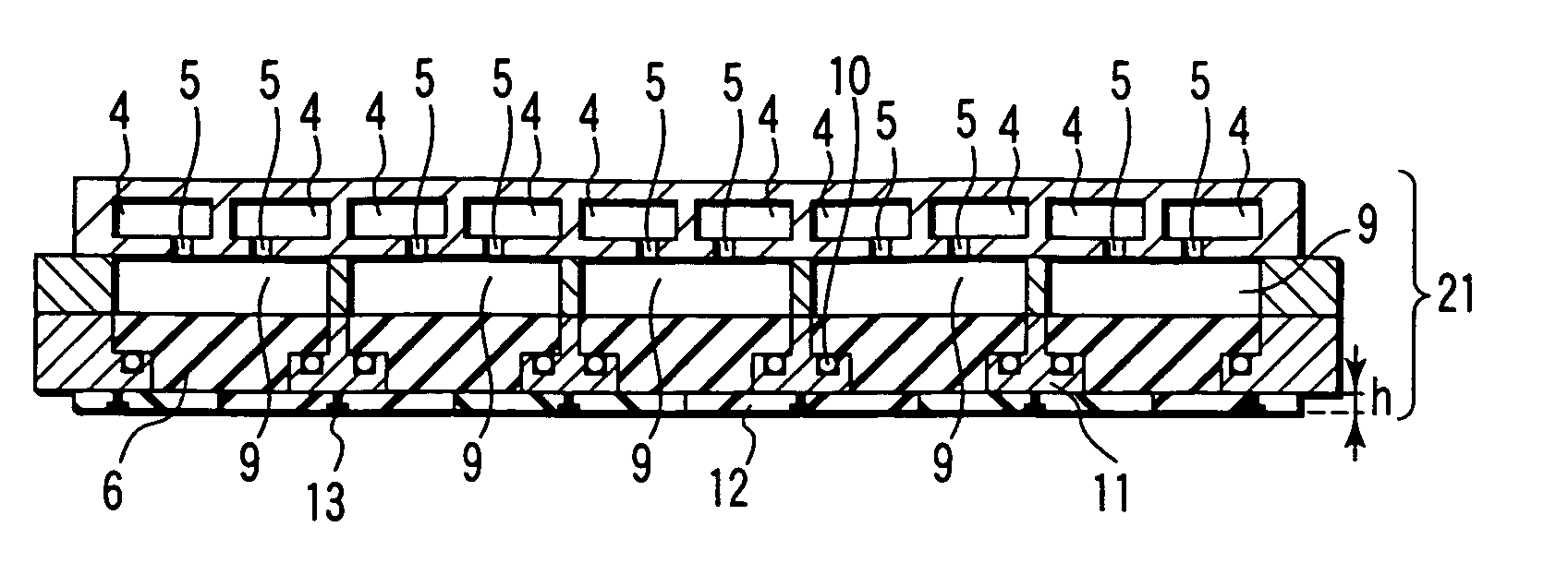
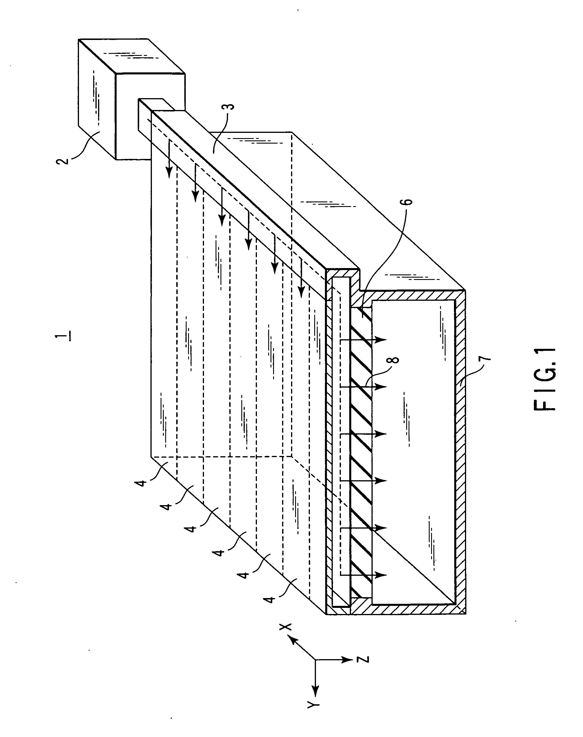
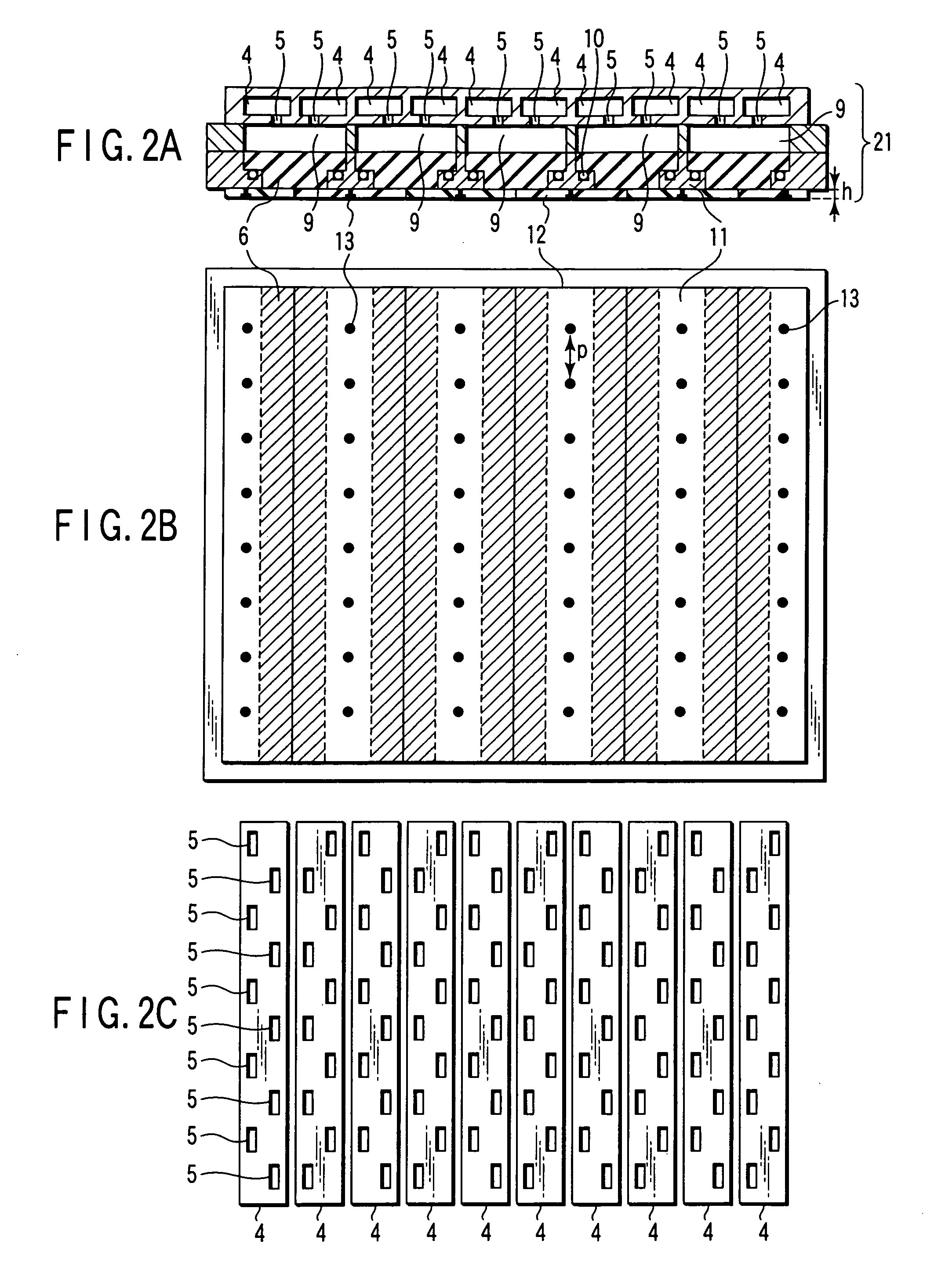
[0060] The state of the plasma 22 at the electromagnetic wave introducing section 21 was examined in detail, and the following result was found. FIG. 5 is a cross-sectional view that shows, in enlarged scale, the region of one dielectric window 6 of the electromagnetic wave introducing section 21 shown in FIG. 2A. Electromagnetic waves that come from the slots 5 enter the dielectric window 6, which is supported by the beams 11, through the cavity portion 9. The electromagnetic waves that have passed through the dielectric window 6 are radiated into the processing chamber 7. Although the electromagnetic waves are radiated to the region just below the dielectric window 6, the electromagnetic waves are not radiated to the region just below the metallic beam 11 since the conductor of the metallic beam 11 is exposed. Consequently, the electromagnetic waves are cut off at the region just below the beam 11. As a result, the uniformity in plasma deteriorates.
[0061] In order to improve the ...
second embodiment
[0080] In a case where the thickness of the quartz plate that is the dielectric plate 12 in the first embodiment was gradually increased to 54 to 60 mm or more, it was observed that the uniformity in plasma light-emission intensity distribution was further improved. In addition, the uniformity in film thickness distribution of a silicon dioxide film, which was formed using the same plasma processing apparatus 1, was measured. FIG. 8 shows measurement results. In FIG. 8, the thicknesses of dielectric plates 12 of quartz and dielectric plates 12 of alumina were gradually increased, and silicon dioxide films were formed under the same conditions. The uniformity in film thickness distribution was plotted on the ordinate, and the thickness of the quartz or alumina plates was plotted on the abscissa.
[0081] To begin with, the result relating to the quartz dielectric plates 12 (indicated by circles in white) is described. When the thickness was set at 30 mm, as mentioned above, good unifor...
third embodiment
[0087] In a third embodiment of the invention, with the attachment of the dielectric plate 12 having a thickness of ½ or more of the wavelength of the electromagnetic wave propagating within the dielectric plate 12, the condition for plasma generation with good uniformity was examined. In FIG. 10, the abscissa indicates the thickness of the dielectric plate 12 and the ordinate indicates an incidence angle α of the electromagnetic wave (see FIG. 5). FIG. 10 shows, by contour lines, the transmittance of electromagnetic waves that are made incident from the dielectric window 6 (quartz dielectric window 6 in this case) on the dielectric plate 12 (quartz dielectric plate 12 in this case).
[0088] That the electromagnetic wave transmittance is close to 1 means that reflection hardly occurs at the interface between the dielectric window 6 and dielectric plate 12 and good propagation of electromagnetic waves occurs in the dielectric plate 12. In the case of the dielectric plate 12 having a t...
PUM
| Property | Measurement | Unit |
|---|---|---|
| Thickness | aaaaa | aaaaa |
| Wavelength | aaaaa | aaaaa |
Abstract
Description
Claims
Application Information