Semiconductor device and method for fabricating thereof
a technology of semiconductor devices and semiconductor films, applied in semiconductor devices, electrical devices, transistors, etc., can solve the problems of reducing device characteristics, affecting the efficiency of the device, so as to reduce the coupling noise in adjacent bits, suppress the generation of residues, and suppress the effect of error generation
- Summary
- Abstract
- Description
- Claims
- Application Information
AI Technical Summary
Benefits of technology
Problems solved by technology
Method used
Image

Examples
first embodiment
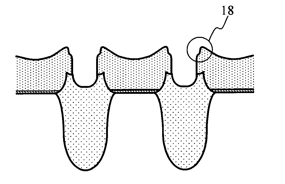
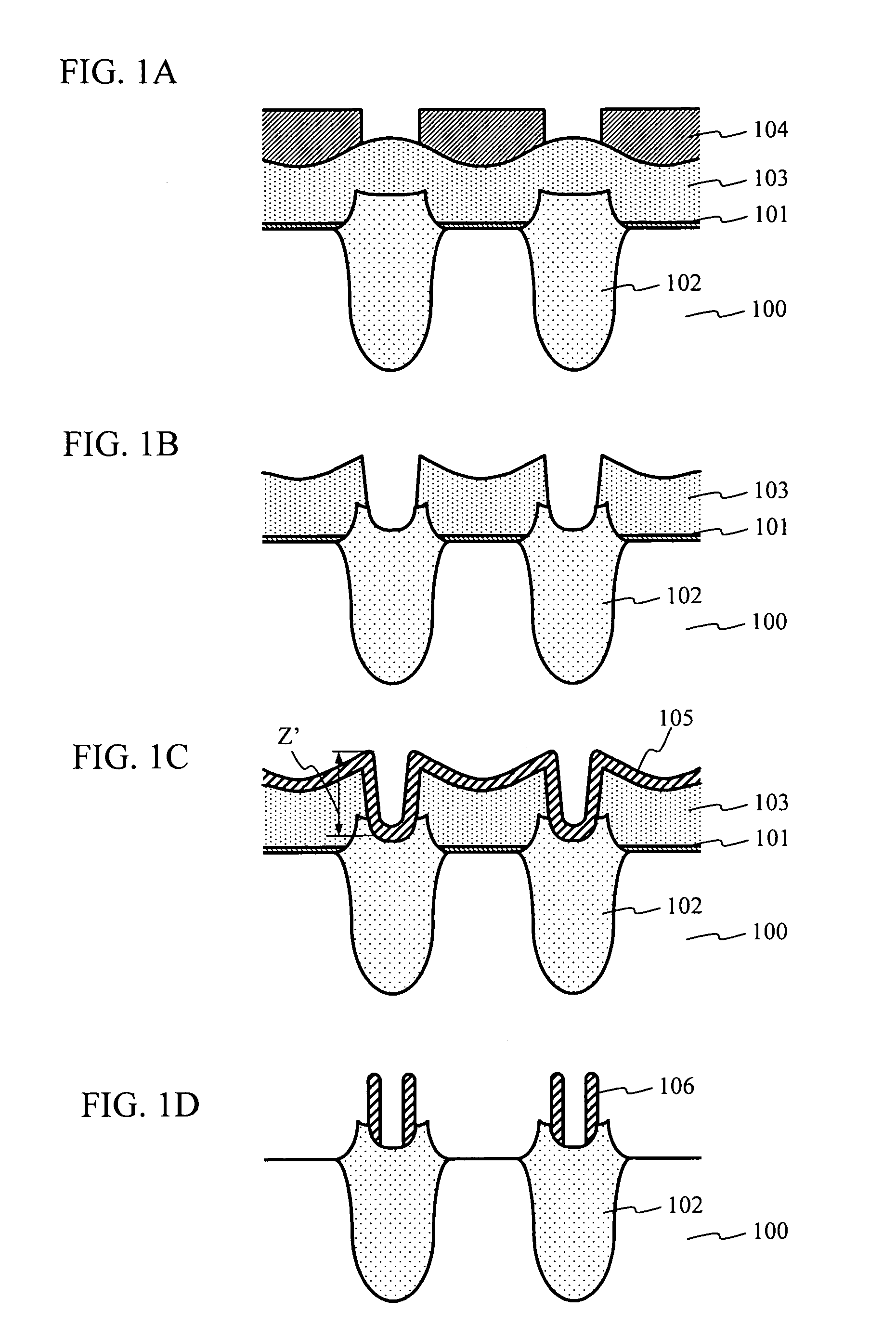
[0035]FIGS. 3A through 3G are views illustrating a first example of a method for fabricating the semiconductor device of the present invention. In the figures, a reference numeral 10 represents the silicon substrate, a reference numeral 11 represents the tunnel oxide film, a reference numeral 12 represents the STI, a reference numeral 13 represents the phosphor doped polysilicon to be formed into the floating gate, a reference numeral 14 represents a first hard mask of a silicon nitride film, a reference numeral 15 represents a photoresist, a reference numeral 16 represents one region of the polysilicon 13 to be removed in the etching process described later, a reference numeral 17 represents a second hard mask of the silicon nitride film, a reference numeral 18 represents a step portion on the polysilicon 13, a reference numeral 19 represents an ONO film of a high dielectric film, and a reference numeral 20 represents polysilicon to be formed into the control gate.
[0036] A descrip...
second embodiment
[0048] In the first embodiment of the present invention, the hard mask made of silicon nitride film is employed for forming the step portion 18 on the sidewall of the polysilicon 13. This step portion may be formed with a general photolithography technique with the use of a photoresist mask.
[0049]FIGS. 4A through 4C are views illustrating a second example of the method for fabricating the semiconductor device of the present invention. In FIGS. 4A through 4C, the same components and configurations as those of the first embodiment have the same reference numerals.
[0050] First, there is formed the tunnel oxide film 11, which is thin and has the thickness of, for example, 75 to 150 Å on a main surface of the semiconductor substrate 10. The activating regions in the respective cells are isolated by The STI (12) formed in a region close to the surface in the semiconductor substrate 10. Then, the tunnel oxide film 11 and the STI (12) are covered with the polysilicon 13 to be formed into ...
third embodiment
[0056] In either the first or second embodiment, another process is not performed in order to apply a special change to the shape of the step after the step portion 18 is formed on the sidewall of the polysilicon 13. However, the step portion 18 of the polysilicon 13 has a sharp angle (corner) in a cross-sectional outline thereof. If this is used as the floating gate in a cell region, the electric filed concentrates on the corner, causing dielectric breakdown in the ONO film 19. In order to avoid the aforementioned dielectric breakdown, it is preferable that the corner of the step portion 18 should be rounded by thermal oxidization after the step portion 18 is formed.
[0057]FIG. 5A through 5C are views illustrating a process for rounding the corner of the step portion 18 by the thermal oxidization. FIG. 5A shows a state in which the silicon nitride film 14 of the first hard mask is removed after the process shown in FIG. 3E is finished. As shown in this figure, after the silicon nit...
PUM
| Property | Measurement | Unit |
|---|---|---|
| height | aaaaa | aaaaa |
| size | aaaaa | aaaaa |
| thickness | aaaaa | aaaaa |
Abstract
Description
Claims
Application Information