Semiconductor device, circuit board, electro-optic device, electronic device

a technology of semiconductor devices and semiconductors, applied in semiconductor devices, semiconductor/solid-state device details, instruments, etc., can solve the problems of weakened adhesion of resin bumps, difficult to break, chemical instability of cu oxides, etc., to achieve the effect of simplifying the manufacturing process and facilitating the etching

Inactive Publication Date: 2006-05-04
SEIKO EPSON CORP
View PDF4 Cites 15 Cited by
  • Summary
  • Abstract
  • Description
  • Claims
  • Application Information

AI Technical Summary

Benefits of technology

[0024] The inventors of the present invention recognized that the etching rate depends on the surface condition of the board. For example, in a case that a resin bump made of epoxy resin is formed on the board made of silicone resin and TiW is plated on that, the TiW plated on the resin bump is etched faster than the TiW plated on the silicone board when etching with hydrogen peroxide. The present invention selectively removes the sacrifice layer, utilizing the difference in etching rate. Because the present invention needs only a single etching of the whole active face to form a space, it makes it possible to simplify the manufacturing process.
[0025] The active face may be made of inorganic material. Because a bigger difference in the surface condition from the resin bump can be made, this makes it possible to carry out the etching more effectively.

Problems solved by technology

Therefore, the conductive layer receives less stress than when it is joined to the resin bump, and it becomes hard to break.
For example, Au usually does not generate any oxide, and Cu oxide is chemically unstable although it is generated.
Therefore, the conductive layer and the resin bump have weakened adhesion.

Method used


Image

  • Semiconductor device, circuit board, electro-optic device, electronic device
  • Semiconductor device, circuit board, electro-optic device, electronic device
  • Semiconductor device, circuit board, electro-optic device, electronic device

Examples


first embodiment

[0050] Electro-Optic Device

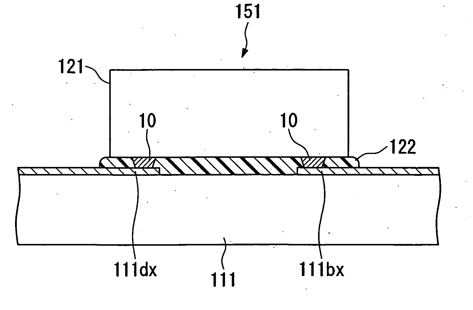
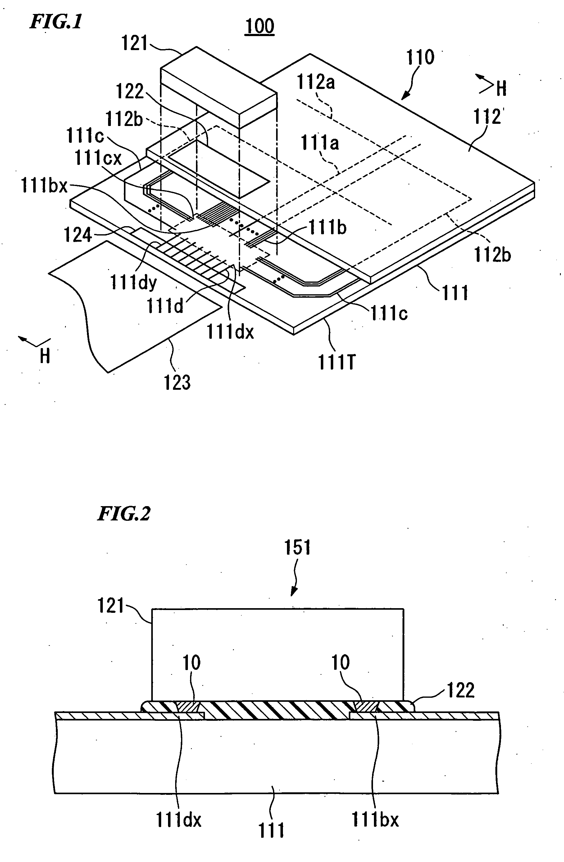
[0051]FIG. 1 is a drawing of a liquid crystal display of an electro-optic device according to an embodiment of the present invention. A liquid crystal display device 100 in FIG. 1 has a liquid crystal panel 110 and a semiconductor element 121 disposed thereon. A deflecting plate, a reflecting sheet, a backlight or other additional portions which are not shown in the drawing are provided as required.

[0052] The liquid crystal panel 110 has a board 111 and a board 112 made of glass or plastic. The board 111 and the board 112 are disposed opposite each other, and are adhered together by a seal which is not shown in the drawing. Liquid crystal made of an electro-optic material is included between the board 111 and the board 112 (not shown in FIG. 1). An electrode 111a made of a clear conductive material such as ITO (Indium Tin Oxide) is formed on the surface inside the board 111, and an electrode 112a which is faced perpendicularly to the electrode 111a is fo...

second embodiment

[0078] A Semiconductor Device.

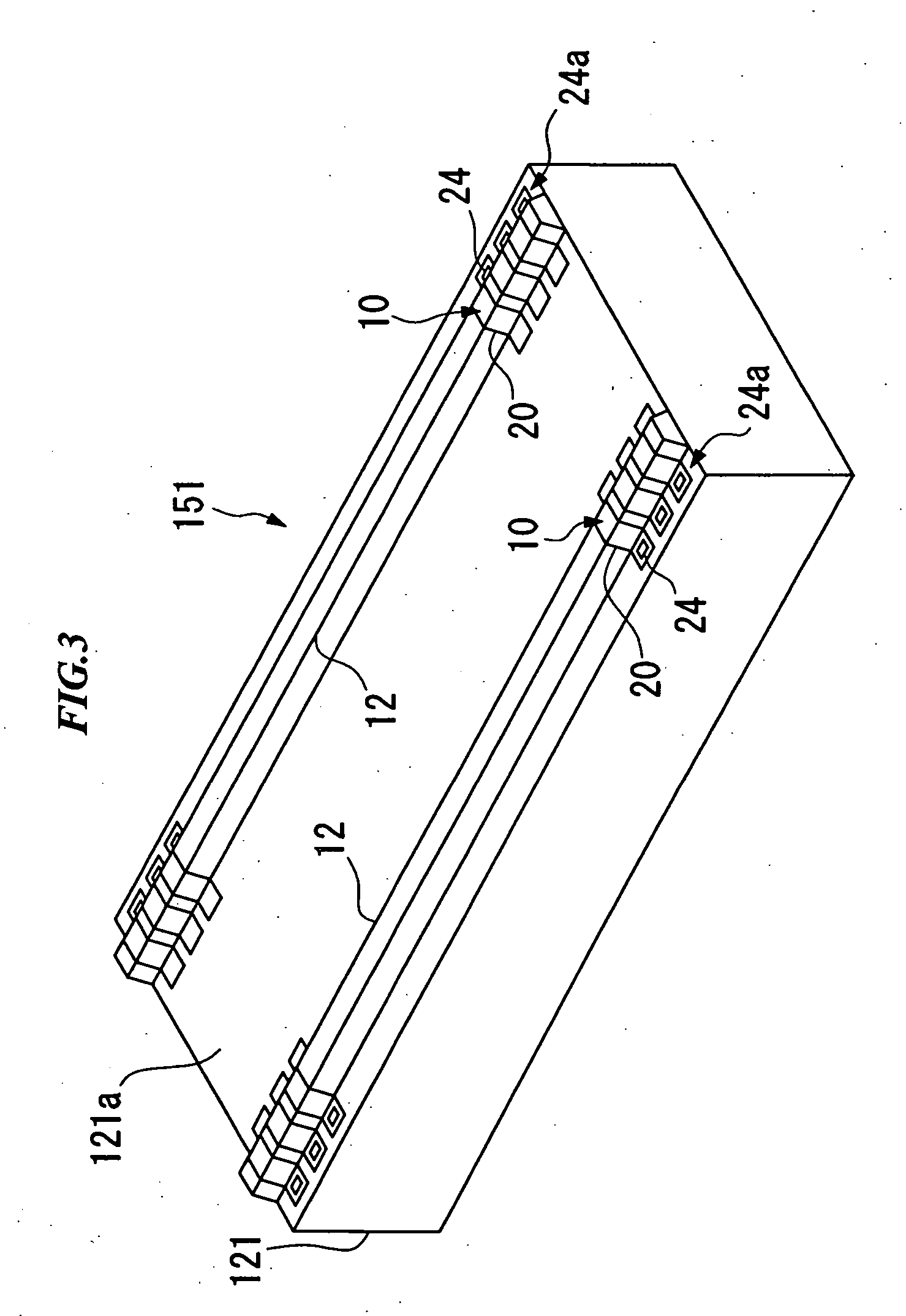
[0079] An explanation on the second embodiment of the present invention is given. FIG. 6 is a drawing showing the main portion of the resin bump electrode 10 of the embodiment. This drawing corresponds to FIG. 4B in the first embodiment.

[0080] The electrode pad, the resin bump, and the passivation layer and several other components in this embodiment have the same structure and arrangement as the first embodiment. Therefore, the same reference number is provided to these common components and portions, and a detailed explanation is omitted.

[0081] In this embodiment, a plurality of conductive layers 22 is formed from the surface of the electrode pad 24 to the surface of the resin bump 12. A barrier metal layer 27 is provided between the conductive layer 22 and the electrode pad 24 so that the metal of the conductive layer 22 does not expand to the electrode pad 24. The barrier metal layer 27 is provided on either side of the resin bump 12. The conduct...


PUM


Abstract

A semiconductor device including a semiconductor element, an electrode pad formed on the semiconductor element, and a bump electrode conductively connected to the electrode pad which includes a resin bump formed on an active face of the semiconductor element and a conductive layer provided from the electrode pad to the surface of the resin bump, the conductive layer and the resin bump being arranged without adhesion.

Description

BACKGROUND OF THE INVENTION [0001] 1. Field of the Invention [0002] The present invention relates to a semiconductor device and its manufacturing method, a circuit board, an electro-optic device and an electronic device. [0003] Priority is claimed on Japanese Patent Application No. 2004-313839, filed Oct. 28, 2004, the content of which is incorporated herein by reference. [0004] 2. Description of Related Art [0005] In circuit boards and liquid crystal displays which are used in various kinds of electric devices, semiconductor devices such as integrated circuit chips (IC chips) are mounted on the boards. For example, in a liquid crystal display, an IC chip for activating a liquid crystal panel is mounted on a glass board (the partner board) which is a component of the liquid crystal panel (a so-called COG structure). In a case in which an IC chip made of hard silicon board is mounted on a hard glass board, it is hard to absorb warpage of the IC chip and the glass board. To solve this...

Claims


Application Information

Patent Timeline
Patent Type & Authority Applications(United States)
IPC IPC(8): H01L23/48H01L23/52
CPCG02F1/13458H01L21/563H01L23/562H01L24/06H01L24/11H01L24/13H01L24/14H01L24/27H01L24/29H01L24/32H01L24/73H01L24/81H01L24/83H01L24/90H01L24/91H01L2224/0231H01L2224/02313H01L2224/0236H01L2224/02377H01L2224/024H01L2224/114H01L2224/116H01L2224/11831H01L2224/13016H01L2224/13099H01L2224/16225H01L2224/27825H01L2224/27831H01L2224/29008H01L2224/29013H01L2224/29017H01L2224/29023H01L2224/2919H01L2224/29191H01L2224/29563H01L2224/2957H01L2224/29582H01L2224/29624H01L2224/29644H01L2224/29647H01L2224/29655H01L2224/29664H01L2224/29666H01L2224/29671H01L2224/29684H01L2224/29695H01L2224/30155H01L2224/73204H01L2224/83101H01L2224/83191H01L2224/83856H01L2924/01002H01L2924/01013H01L2924/01022H01L2924/01029H01L2924/01033H01L2924/01046H01L2924/01049H01L2924/0105H01L2924/01074H01L2924/01078H01L2924/01079H01L2924/01082H01L2924/14H01L2924/3511H01L2924/0132H01L2924/01005H01L2924/01006H01L2924/01019H01L2924/01024H01L2924/01066H01L2924/014H01L2924/0665H01L2224/29101H01L2224/0233H01L2224/0239H01L2224/32225H01L2224/13666H01L2224/1319H01L2224/13644H01L2224/13647H01L2224/13655H01L2224/13664H01L2224/13671H01L2224/13684H01L2224/13624H01L2924/0001H01L2224/0401H01L2924/00014H01L2924/01023H01L2924/00H01L2924/01028H01L2924/01084H01L2224/131H01L23/48
Inventor TANAKA, SHUICHI
Owner SEIKO EPSON CORP
Why Eureka
Try Eureka