Method of analyzing operation of semiconductor integrated circuit device, analyzing apparatus used in the same, and optimization designing method using the same

Inactive Publication Date: 2006-05-04
PANASONIC CORP
View PDF7 Cites 116 Cited by
  • Summary
  • Abstract
  • Description
  • Claims
  • Application Information

AI Technical Summary

Benefits of technology

[0063] As described above, according to the invention, the impedance of the substrate is considered in the analysis of the power noise of the semiconductor integrated circuit. Therefore, it is poss

Problems solved by technology

However, it is impossible to disregard the influence of a slight simulation error on the delay of each element due to an enhancement in the degree of an integration.
Although the amount of a calculation is large, the same information is insufficient for carrying out an analysis with high precision.
In addition to an enhancement in the degree of an integration, however, the influence of the slight deviation of a logical simulation on a delay cannot be disregarded, and the logical simulation with high precision is required in respect of the analysis of an operation.
Refer

Method used


Image

  • Method of analyzing operation of semiconductor integrated circuit device, analyzing apparatus used in the same, and optimization designing method using the same
  • Method of analyzing operation of semiconductor integrated circuit device, analyzing apparatus used in the same, and optimization designing method using the same
  • Method of analyzing operation of semiconductor integrated circuit device, analyzing apparatus used in the same, and optimization designing method using the same

Examples


first embodiment

[0093] (First Embodiment)

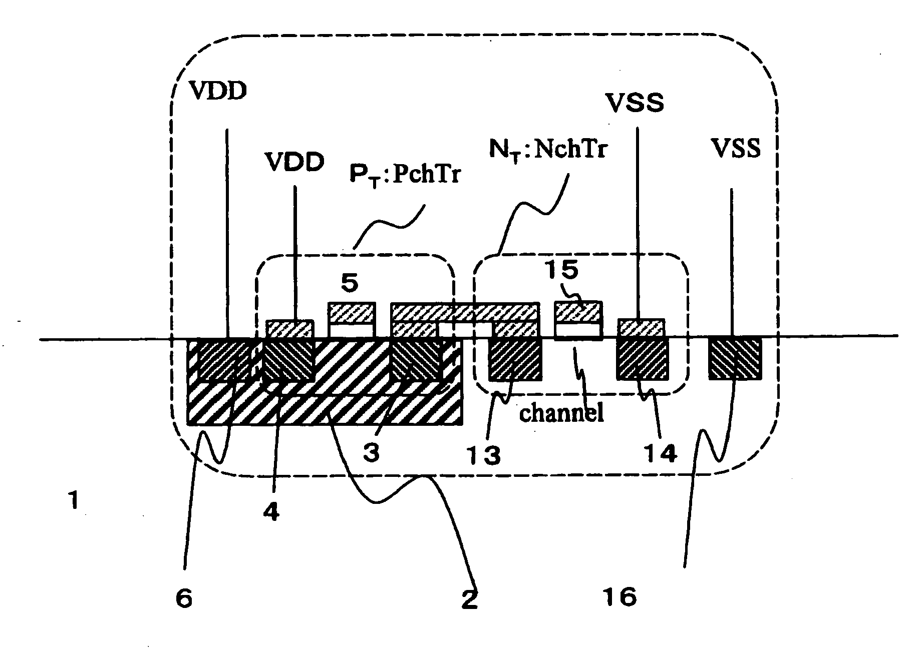
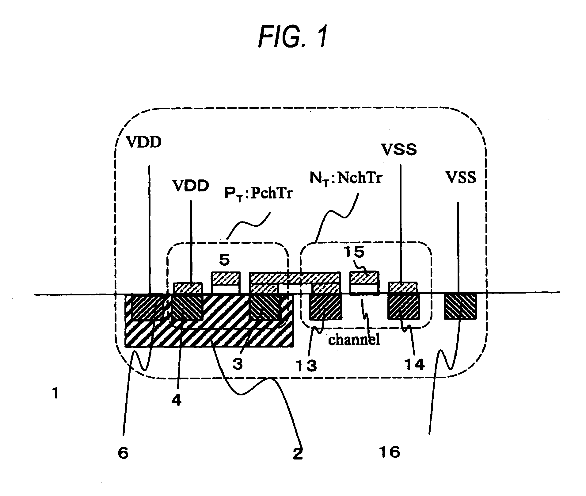
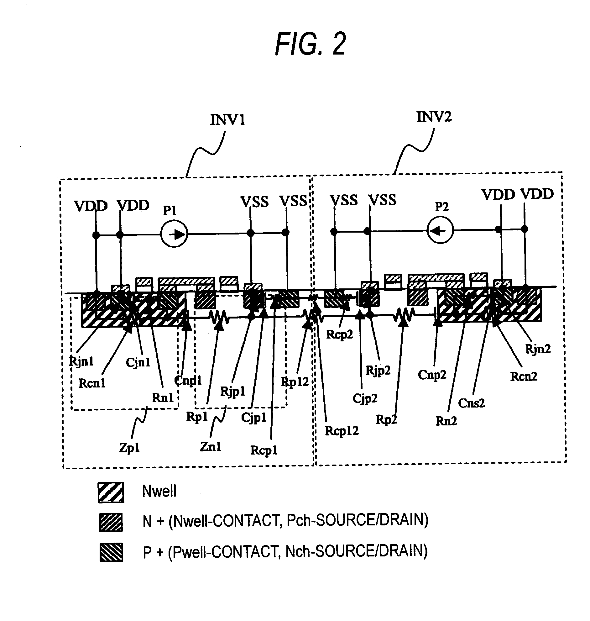
[0094] FIGS. 1 to 3 are principle diagrams showing a procedure for analyzing a power noise according to the embodiment.

[0095] A method of analyzing a power noise of a semiconductor integrated circuit according to the embodiment of the invention is characterized in that a transistor is replaced with a current source Ps as in a related analyzing method (see FIG. 25), and furthermore, a semiconductor integrated circuit including a transistor shown in FIG. 1 is analyzed by using a model considering the impedance of a substrate (structures provided under a metal layer, for example, a P-type substrate or an N-type substrate, a well and a diffusion region are generally referred to as the substrate) as shown in FIG. 2. More specifically, the method is characterized in that modeling is carried out as a combination of an N-type diffusion resistance Rjn, a P-type diffusion resistance Rjp, a junction capacitance Cjn of an N-type diffusion region, a junction capacitance...

second embodiment

[0112] (Second Embodiment)

[0113] Next, description will be given to an example in which the inside of a substrate is divided into meshes and modeling is carried out by an equivalent circuit according to a second embodiment of the invention.

[0114] While the description has been given to the example in which the diffusion regions are connected through the equivalent RC net in the first embodiment, description will be given to an example in which the substrate is divided into three-dimensional meshes to carry out the modeling in the embodiment.

[0115]FIG. 6 is a flowchart showing the embodiment, and FIG. 7 is a diagram in which the impedance of the substrate 1 (see FIG. 1) used in the first embodiment is divided into meshes and is thus modeled.

[0116] Layout information 501 is used for circuit information as shown in FIG. 5 and an impedance is calculated for each mesh by substrate mesh impedance calculating means 502, thereby forming a substrate net list 503. A broken line in an N wel...

third embodiment

[0122] (Third Embodiment)

[0123] In a third embodiment according to the invention, next, description will be given to a method of analyzing a power noise in which a division into meshes is carried out on the basis of a contact position, thereby performing modeling. In this example, the division into meshes is carried out on the basis of the contact position, thereby performing the modeling in place of modeling between points as shown in an explanatory diagram of FIG. 8.

[0124] A division into meshes passing through a contact 6 (a point P1) to an N well 2 and a contact 16 (a point P2) to a P substrate is carried out to perform the modeling.

[0125] For example, a contact is formed in the position of a diffusion region on the basis of the position of the diffusion region in many cases. Therefore, it is possible to easily carry out an analysis on the basis of the contact position.

[0126] When the contact is thus set to be the basis, moreover, existing means such as an LPE tool can easily...


PUM


Abstract

In a method of analyzing a power noise based on the circuit information of a semiconductor integrated circuit device, the power noise is analyzed in consideration of the influence of the impedance of a substrate. Consequently, the impedance of the substrate which has not been conventionally considered is taken into consideration. Thus, precision in the analysis can be enhanced more greatly.

Description

[0001] This application is based on Japanese Patent Application No. 2004-287544, which is incorporated herein by reference. BACKGROUND OF THE INVENTION [0002] 1. Field of the Invention [0003] The present invention relates to a method of analyzing the operation of a semiconductor integrated circuit device, an analyzing apparatus to be used in the method, and an optimization designing method using the apparatus, and more particularly to a method of analyzing an operation at a high speed with high precision for a large scale and high-speed driving LSI (a large scale semiconductor integrated circuit). [0004] 2. Description of the Related Art [0005] In a design for a semiconductor integrated circuit, usually, it is important that a timing is analyzed as to whether a timing between flip-flops is matched, thereby carrying out an optimization. For this reason, there has been employed a method of analyzing the operation of a circuit, calculating a delay value and carrying out an optimum desi...

Claims


Application Information

Patent Timeline
IPC IPC(8): H01L23/52
CPCG06F17/5031G06F30/3312
Inventor SHIMAZAKI, KENJISATOH, KAZUHIROTSUJIKAWA, HIROYUKIHIRANO, SHOUZOUNAGATA, MAKOTO
Owner PANASONIC CORP
Why Eureka
Try Eureka