Nanopatterning method

a technology of nano-patterning and patterning, applied in the direction of material nanotechnology, coating, electric shock equipment, etc., can solve the problems of generating noise patterns and limited methods to micro-size patterns

Inactive Publication Date: 2006-05-04
SEOUL NAT UNIV R&DB FOUND
View PDF1 Cites 23 Cited by
  • Summary
  • Abstract
  • Description
  • Claims
  • Application Information

AI Technical Summary

Benefits of technology

[0005] Accordingly, it is an object of the present invention to provide a method for nanopatterning without generating a noise pattern by guiding the migration of diffusive nanoparticles in an efficient manner.

Problems solved by technology

The conventional method cannot adequately control the great diffusive force of nanoparticles having an average size of less than 100 nm, resulting in the adherence of a significant portion of the nanoparticles to the region beside the formed pattern to generate a noise pattern.
However, this method is limited to micron-size patterning.

Method used


Image

  • Nanopatterning method
  • Nanopatterning method
  • Nanopatterning method

Examples


example 1

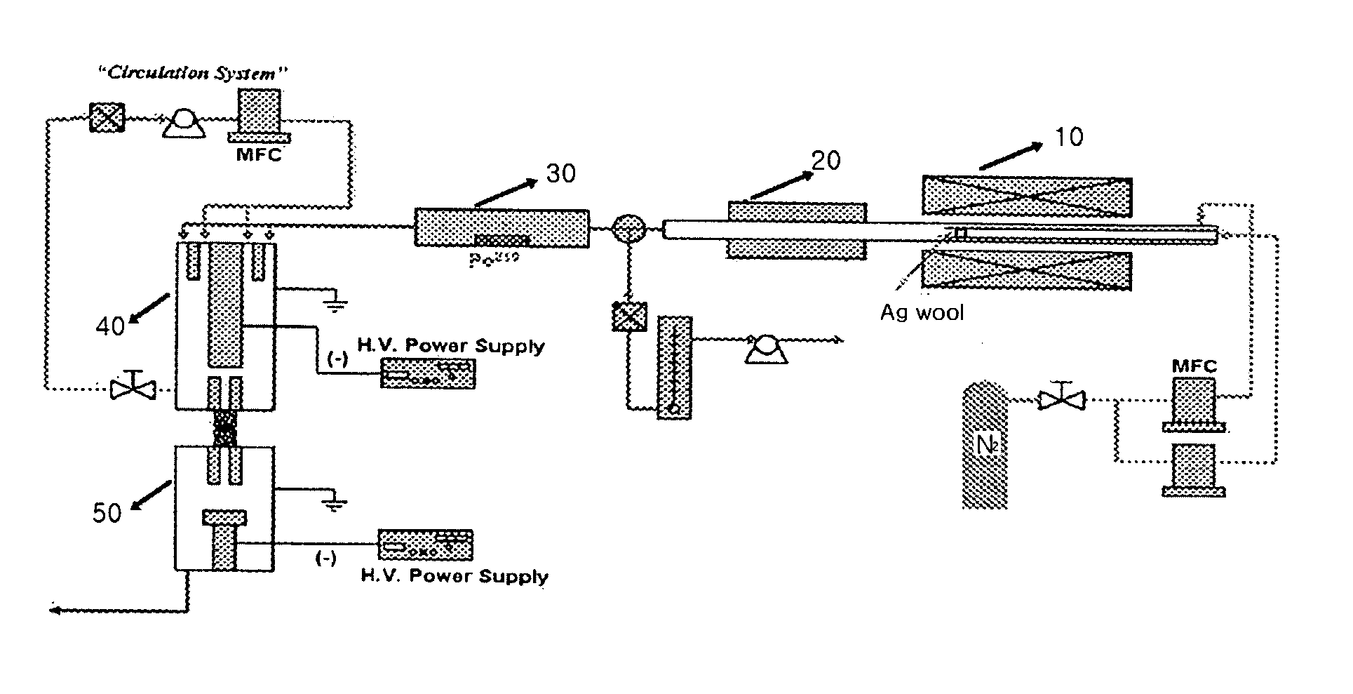
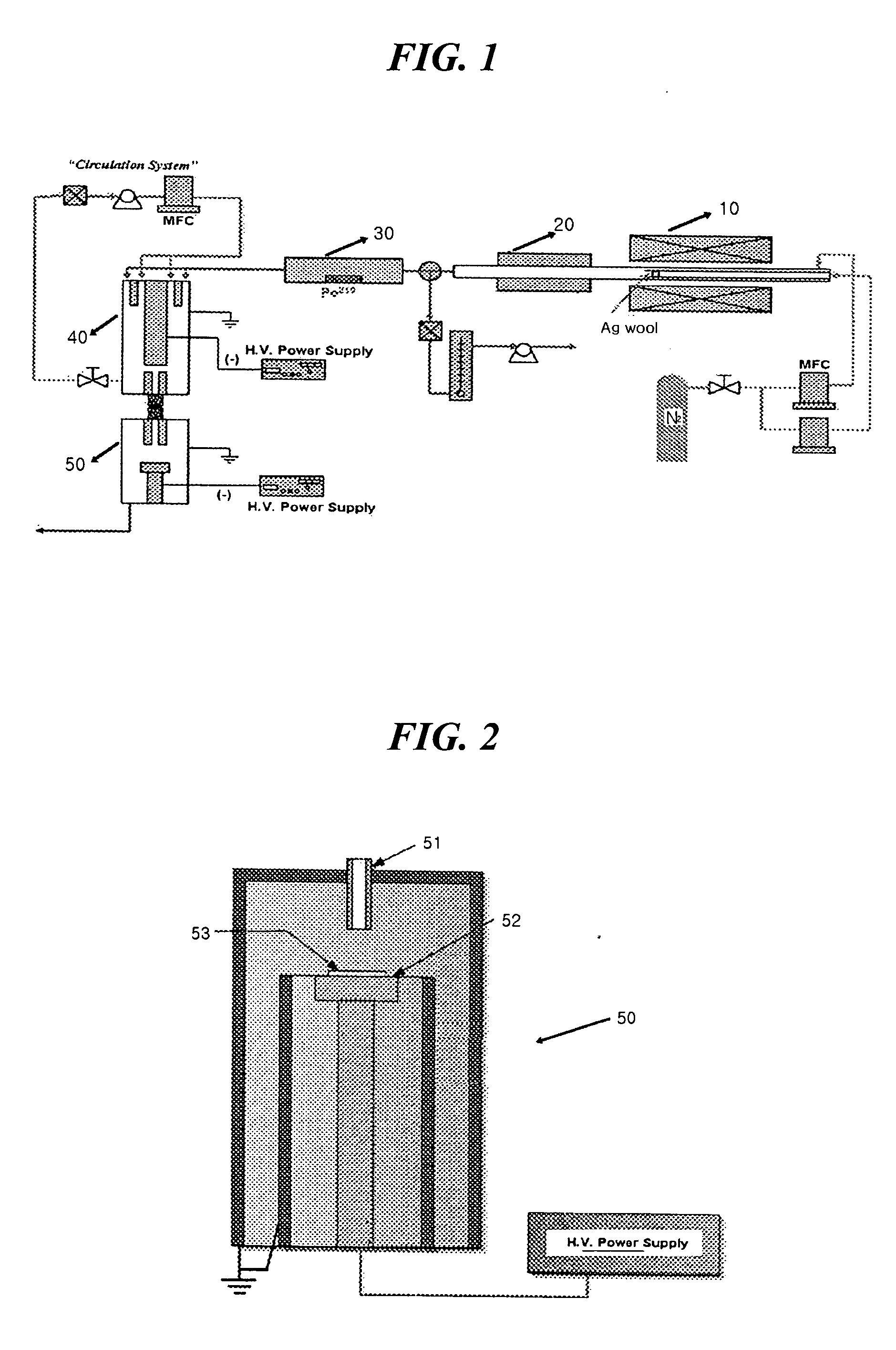
[0022] Nanopatterning was performed by a process illustrated in FIG. 1 using an electrostatic precipitator illustrated in FIG. 2.

[0023] First, a pattern having a line resolution of 100 to 1500 nm was formed on a p-type silicon plate by spin coating a photoresist on a cleaned plate and exposing the photoresist coating layer to ultraviolet or electronic beam-lithograph and removing the exposed region. The patterned plate (53) was placed on copper electrode (52) of electrostatic precipitator (50) and a voltage of −4.5 kV was applied on the copper electrode.

[0024] Subsequently, Ag wool was charged in tubular reactor (10) and Ag particles generated therein were passed through a condenser (20) using a nitrogen carrier gas and a sheath gas at a flow rate of 1200 and 890 cc / min, respectively, to generate polydispersive Ag nanoparticle aerosol, which was introduced to bipolar-charger (30) using radioactive 210-polonium and passed through DMA (40) to which a voltage of −810 V was applied, t...

example 2

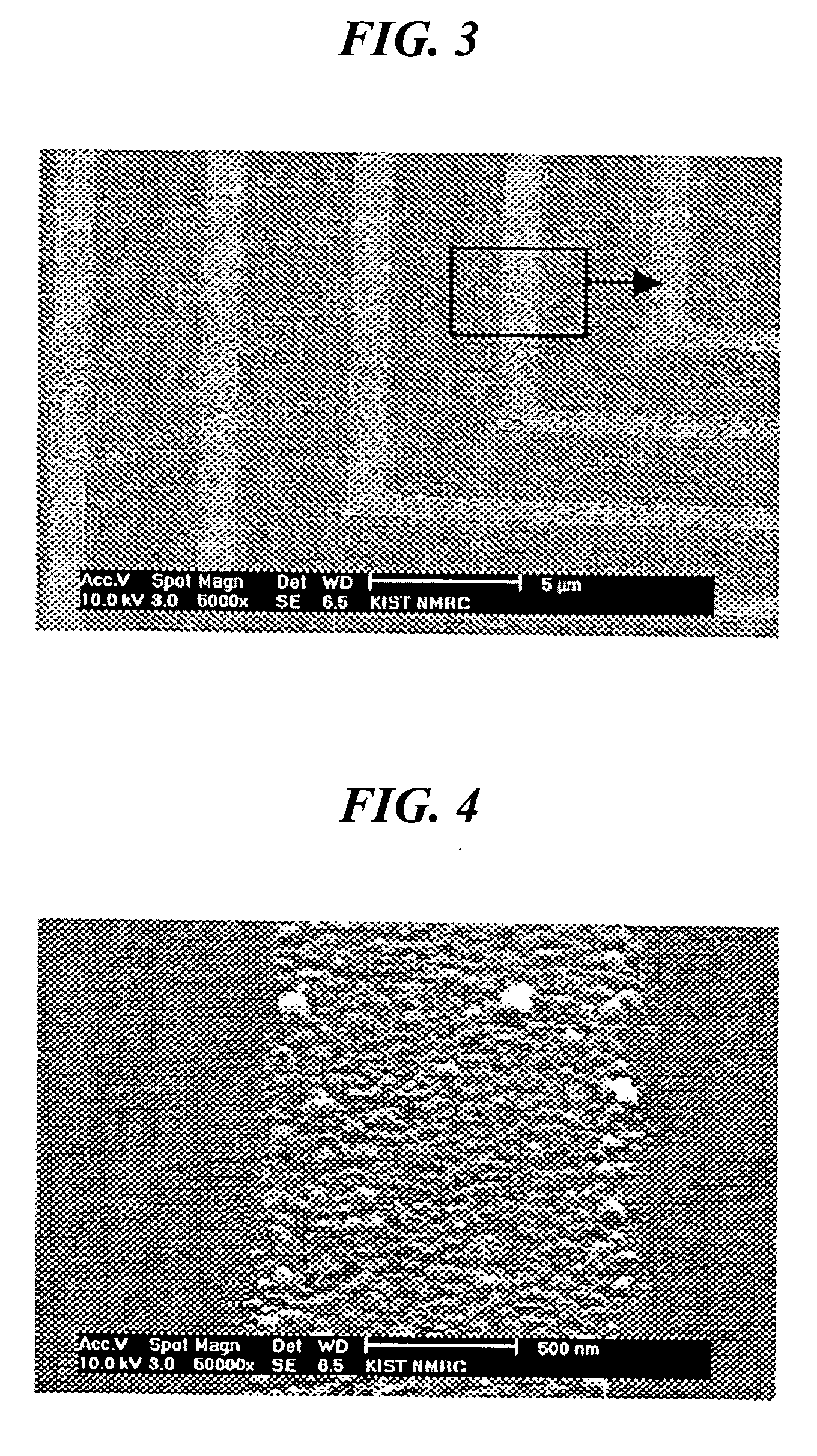
[0028] A 500 nm-diameter dot structure obtained by the procedure of Example 1 was annealed at about 400° C. for about 120 minutes to prepare a sintered structure. SEM and SPM photographs of the sintered structure are shown in FIGS. 7 and 8, respectively.

[0029] As can seen in FIGS. 7 and 8, the sintered structure prepared by the inventive method has a line resolution of about 300 nm which is higher than that obtainable by a conventional method by 40%.

[0030] As described above, in accordance with the present invention, the nanopatterning may be carried out in a high precision and efficiency.


PUM


Abstract

A nano-sized structure can be accurately patterned with no significant noise generation by the inventive method which comprises the steps of (i) placing a plate having a nano-scale pattern formed thereon on the electrode of an externally grounded electrostatic precipitator and applying a voltage on the electrode, and (ii) introducing bipolar-charged monodispersive nanoparticles into the electrostatic precipitator together with a carrier gas and guiding the migration of the bipolar-charged nanoparticles to said pattern on the plate, by the action of an electric field generated by the applied and grounded voltage difference generated in the electrostatic precipitator.

Description

FIELD OF THE INVENTION [0001] The present invention relates to a nanopatterning method which generates no significant noise. BACKGROUND OF THE INVENTION [0002] The formation of a micro- or nano-sized structure by way of manipulating nanoparticles to selectively adhere to a pre-designed pattern is termed nanopatterning, which can be advantageously used for the manufacture of quantum devices, single electron transistors, tera-level memory devices, high performance gas sensers, etc. [0003] Such nanopatterning has been conventionally performed by guiding nanopaticles to a pattern formed on a plate using a means such as a laser, electronic beam, ion beam, scanning probe microscope tip and metal tip. The conventional method cannot adequately control the great diffusive force of nanoparticles having an average size of less than 100 nm, resulting in the adherence of a significant portion of the nanoparticles to the region beside the formed pattern to generate a noise pattern. [0004] Another...

Claims


Application Information

Patent Timeline
Patent Type & Authority Applications(United States)
IPC IPC(8): B05D1/04
CPCB82Y10/00B82Y30/00H01L21/76838
Inventor KIM, HYOUNG CHULCHOI, MAN SOO
Owner SEOUL NAT UNIV R&DB FOUND
Why Eureka
Try Eureka