In-place bonding of microstructures

Inactive Publication Date: 2006-05-04
IBM CORP
View PDF19 Cites 35 Cited by
  • Summary
  • Abstract
  • Description
  • Claims
  • Application Information

AI Technical Summary

Benefits of technology

[0012] The method of the present invention, which has been broadly described above, has the following advantages over conventional wafer bonding methods: The bonding of two wafers and the layer transfer process is replaced in the present invention by progressive layer translation and bonding, all which are done at room temperature. Moreover, the inventive process is

Problems solved by technology

Wafer bonding carried out by the techniques discussed above presents many challenges.
Particles can substantially impact t

Method used


Image

  • In-place bonding of microstructures
  • In-place bonding of microstructures
  • In-place bonding of microstructures

Examples


example 1

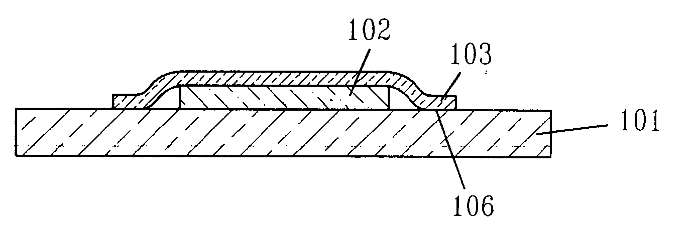
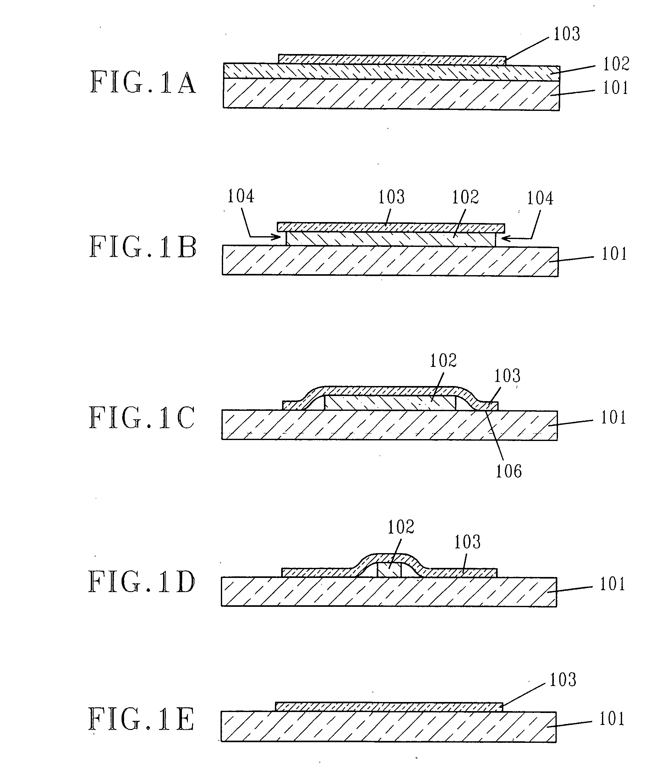
[0043]FIG. 8A shows a scanning electron microscope (SEM) image of a cross section through a micro-slab for which the etching was incomplete (corresponding to FIG. 1C of the invention). The SOI thickness was 55 nm and the buried oxide was 145 nm. The total micro-slab size was about 5×5 microns. The edges of the slab were bonded to the substrate while the center part lies on the unetched portion of the buried oxide.

[0044]FIG. 8B shows a tilted view, SEM image of a sample for which the etching of the buried oxide was completed. The micro-slabs were 8.5×8.5 microns in size. The SOI thickness was 55 nm. As can be seen and was further confirmed by Atomic Force microscope (AFM) measurements, the micro-slabs lied flat on the substrate. Additionally, the micro-slabs maintained their exact relative position as was before the buried oxide was etched away. The edge of the sample was obtained by cleaving the wafer into two parts. The wafer was not annealed, so the micro-slabs were held to the s...

example 2

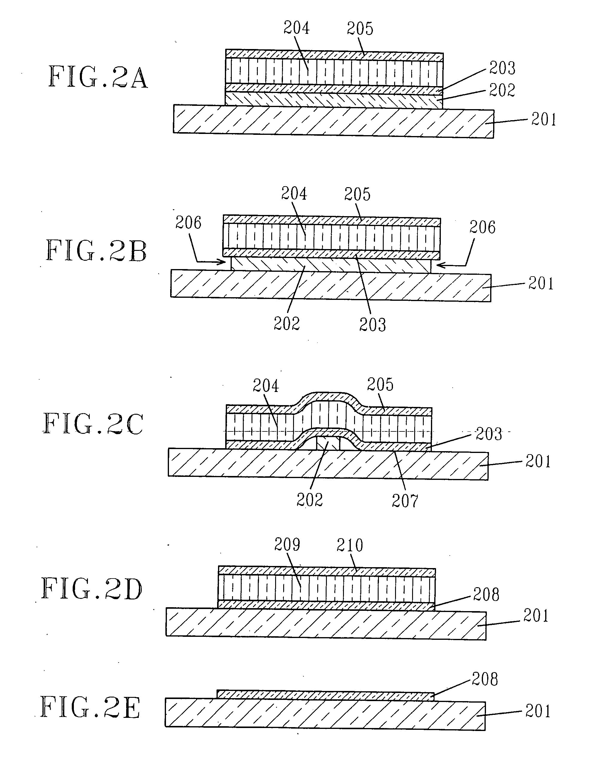
[0045]FIG. 8C shows an SEM image of an array of micro-slabs having a gear shape that were bonded using the in-place bonding technique of the present invention. Each micro-slab consisted of a tri-layer film stack of Si / SiGe / Si. The total film stack thickness was about 340 nm with each Si film being about 20 nm thick. The Ge concentration in the SiGe alloy was about 20%. As discussed earlier, the micro-slabs maintained their exact relative position as was before the etching of the buried oxide. The image corresponds to the process step shown in FIG. 2D of the present invention. During the buried oxide etch, the strain in the SiGe film transfered to the top and bottom Si layers. The strain transfer was verified by a high-resolution x-ray diffraction (HRXRD) measurement of the sample, which measures the Bragg angle, θB corresponding to the out-of-plane lattice constant of the different layers in the structure. FIG. 8D shows a 004 diffraction map of the sample shown in FIG. 8C. As can be...


PUM


Abstract

A method for bonding microstructures to a semiconductor substrate using attractive forces, such as, hydrophobic, van der Waals, and covalent bonding is provided. The microstructures maintain their absolute position with respect to each other and translate vertically onto a wafer surface during the bonding process. The vertical translation of the micro-slabs is also referred to herein as “in-place bonding”. Semiconductor structures which include the attractively bonded microstructures and substrate are also disclosed.

Description

FIELD OF THE INVENTION [0001] The present invention relates to semiconductor substrates, and more particularly to a semiconductor substrate having bonded microstructures. The microstructures within the inventive semiconductor substrates can incorporate strained films or different crystal orientation than that of the substrate. The microstructures are formed prior to their bonding to the substrate. BACKGROUND OF THE INVENTION [0002] In the semiconductor industry, wafer bonding is conventionally performed by methods where a first substrate is bonded to a second substrate and then the bulk of the first substrate is removed leaving a thin layer from the first substrate on the surface of the second substrate. The first substrate is usually referred to as the donor wafer, while the second substrate is referred to as the handle wafer. The transfer of the thin film from the donor wafer to the handle wafer can be achieved by known methods such as wafer back grinding, or hydrogen blistering (...

Claims


Application Information

Patent Timeline
IPC IPC(8): H01L21/337H01L21/331
CPCH01L24/26H01L24/83H01L2924/1306H01L2924/0132H01L2924/01072H01L2924/01023H01L25/16H01L25/50H01L2224/8385H01L2224/83894H01L2924/01005H01L2924/01011H01L2924/01013H01L2924/01015H01L2924/01032H01L2924/01033H01L2924/07802H01L2924/13091H01L2924/01006H01L2924/01019H01L2924/01014H01L2924/00
Inventor COHEN, GUY MOSHEMOONEY, PATRICIA M.PARUCHURI, VAMSI K.
Owner IBM CORP
Why Eureka
Try Eureka