

Class of bridged biphenylene polymers
a technology of biphenylene polymer and polymer, which is applied in the field of bridged biphenylene polymer, can solve the problems of low efficiency, energy transfer from the excited emissive compound, and the major obstacle to their commercial application, and achieve the effect of improving brightness and/or lifetim
Inactive Publication Date: 2006-05-04
SUMITOMO CHEM CO LTD
View PDF34 Cites 32 Cited by
- Summary
- Abstract
- Description
- Claims
- Application Information
AI Technical Summary
Benefits of technology
[0014] In yet another aspect, practice of the present invention provides OLED and p-OLED devices with improved brightness and / or lifetime.
Problems solved by technology
One cause of low efficiency is energy transfer from the excited emissive compound (whether it be fluorescent or phosphorescent, small molecule or polymer) to a material having a lower energy excited state.
The decreasing brightness of OLEDs and p-OLEDs as a function of time is the major obstacle to their commercial application.
Such chemical reactions may alter the electronic properties of the emissive layer and can lead to decreases in brightness, decreases in efficiency, and (ultimately) device failure.
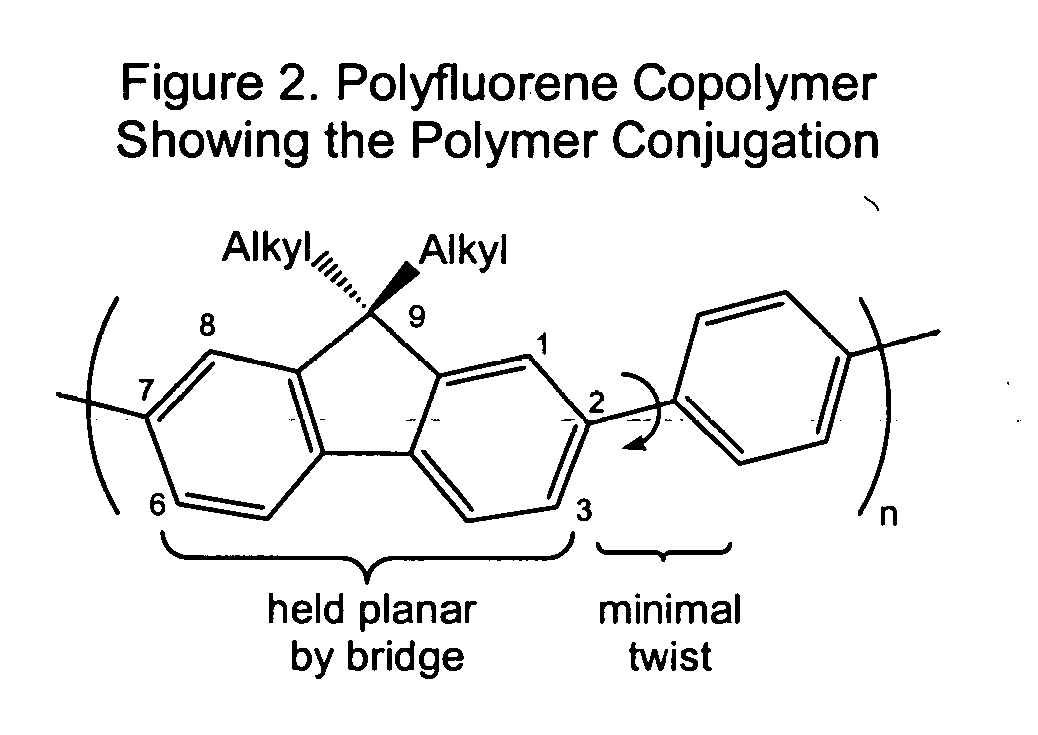
Even the most promising p-OLED materials are limited by short lifetimes. For example, copolymers of methylene-bridged polyphenylenes (polyfluorenes,
In fact, the lifetimes of the best polyfluorene blue phosphors are not suitable for commercial p-OLED applications.
Method used
View moreImage
Smart ImageViewing Examples

Examples
example 11
P-OLED Devices From Polymers 29, 31, 34, and 44
[0225] Standard polymer organic light emitting devices are fabricated by depositing a layer of Baytron P® (Bayer) polyethylenedioxythiophene / polystyrene sulfonate onto a cleaned, ITO coated, pane of glass, followed by spin coating a layer of the polymer (29, 31, 34, or 44) to a thickness of about 100 nm, followed by vacuum evaporation of a 5 nm layer of CsF, followed by vacuum evaporation of a 1 micron layer of aluminum. Devices using polymers 29, 31, and 44 emit blue light, and the device using polymer 34 emits green light on application of a voltage of 5 to 10 V.
Login to View More PUM
| Property | Measurement | Unit |
|---|---|---|
| brightness | aaaaa | aaaaa |
| brightness | aaaaa | aaaaa |
| singlet energy | aaaaa | aaaaa |
Abstract
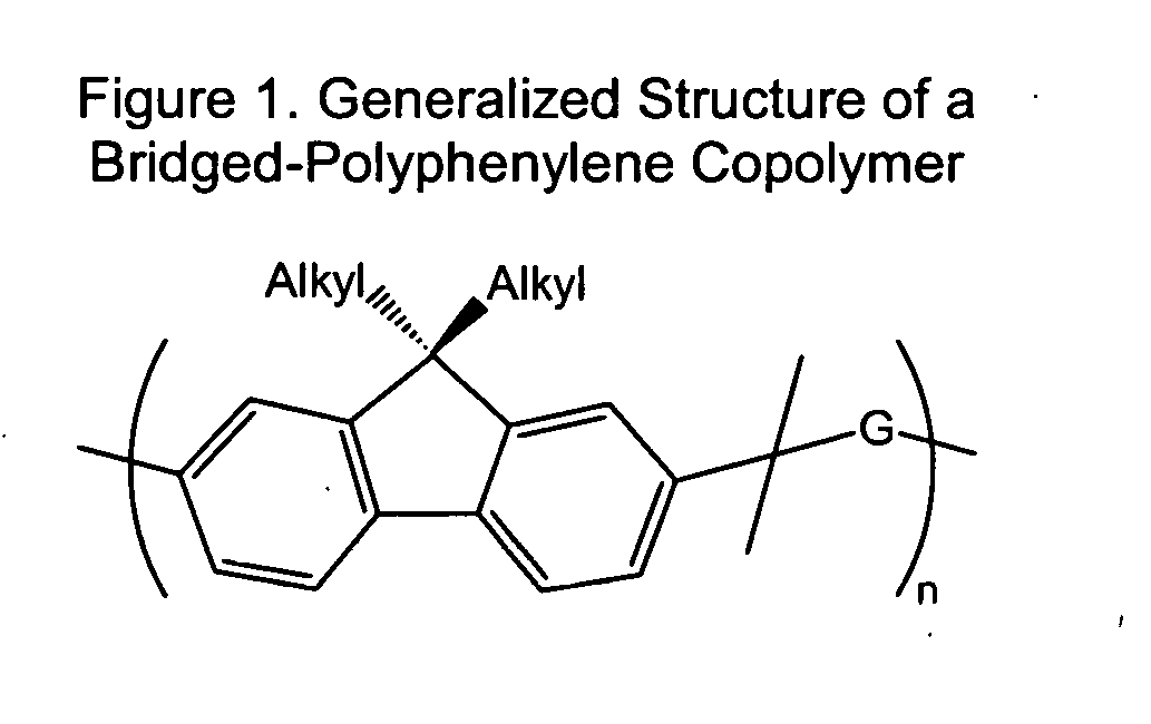
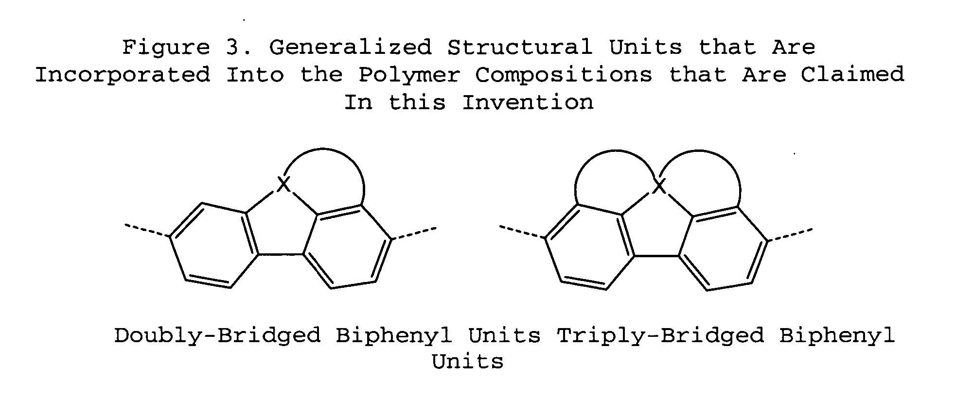
Luminescent polymers having doubly- or multiply-bridged biphenylene repeat units are provided, which are particularly suited as electroluminescent polymers. Monomers necessary for the synthesis of the multiply bridged biphenylene polymers are provided, as are electroluminescent devices utilizing these polymers.
Description
CROSS-REFERENCE TO RELATED APPLICATION(S) [0001] This is an ordinary application of U.S. Provisional Application Ser. No. 60 / 625,047, filed on Nov. 3, 2004, the content of which is expressly incorporated herein by reference as if set forth in full herein.BACKGROUND OF INVENTION [0002] Organic Light Emitting Diodes (OLEDs) are useful in electronic displays, building lighting, signage, and other applications where efficient, lightweight, thin form-factor light sources are needed. An OLED is formed by sandwiching a fluorescent or phosphorescent organic film between two electrodes, at least one of which is transparent. Holes from the anode and electrons from the cathode recombine in the organic film and produce light. If the organic film is a polymer film the device is a polymer-OLED or p-OLED. It is known in the art how to improve efficiency of OLEDs and p-OLEDs by inclusion of various other layers in the sandwich structure, including but not limited to hole injection layers, hole tran...
Claims
Login to View More Application Information
Patent Timeline
 Patent Type & AuthorityApplications(United States)
IPC IPC(8): C08G61/00C09K11/06H01L51/54H05B33/14H01L31/0256H01L33/00H01L33/02H01L33/26H01L33/42
CPCC08G61/10Y10T428/10C08G61/124C09K11/06C09K2211/1416C09K2211/1425H01L51/0035H01L51/0036H01L51/0039H01L51/0043H01L51/0052H01L51/0059H01L51/0062H01L51/0081H01L51/0085H01L51/0089H01L51/5012H01L51/5293Y02E10/549C08G61/123C09K2323/00H10K85/115H10K85/113H10K85/111H10K85/151H10K85/615H10K85/649H10K85/631H10K85/351H10K85/324H10K85/342H10K50/11H10K50/868C08G61/00H01L31/0256H05B33/14C08G61/12
InventorMARROCCO, MATTHEWLEE, VIRGIL
OwnerSUMITOMO CHEM CO LTD