Carbide nanostructures and methods for making same

a carbide nanotube and nanostructure technology, applied in the field of nanostructure making methods, can solve the problems of carbon nanotubes, limited device life and effectiveness, and relatively high work function

Active Publication Date: 2006-05-11
GENERAL ELECTRIC CO
View PDF4 Cites 30 Cited by
  • Summary
  • Abstract
  • Description
  • Claims
  • Application Information

AI Technical Summary

Problems solved by technology

Carbon nanotubes, however, exhibit a fairly high work function, and are prone to damage under typical operating conditions, limiting the life

Method used


Image

  • Carbide nanostructures and methods for making same
  • Carbide nanostructures and methods for making same
  • Carbide nanostructures and methods for making same

Examples


Embodiment Construction

[0028] A preferred embodiment of the invention is now described in detail. Referring to the drawings, like numbers indicate like parts throughout the views. As used in the description herein and throughout the claims, the following terms take the meanings explicitly associated herein, unless the context clearly dictates otherwise: the meaning of “a,”“an,” and “the” includes plural reference, the meaning of “in” includes “in” and “on.” Unless otherwise specified herein, the drawings are not necessarily drawn to scale.

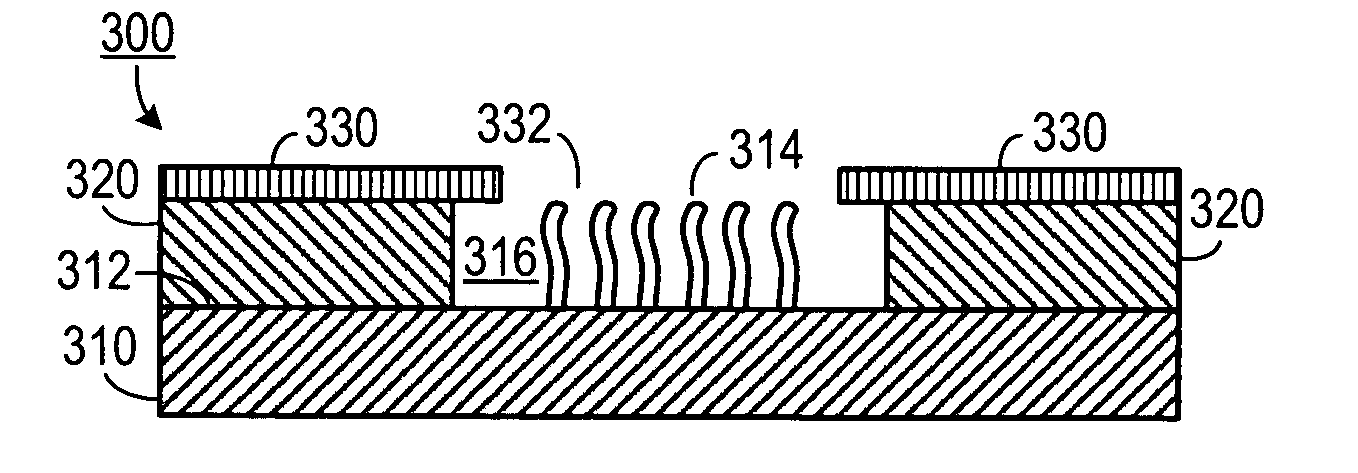
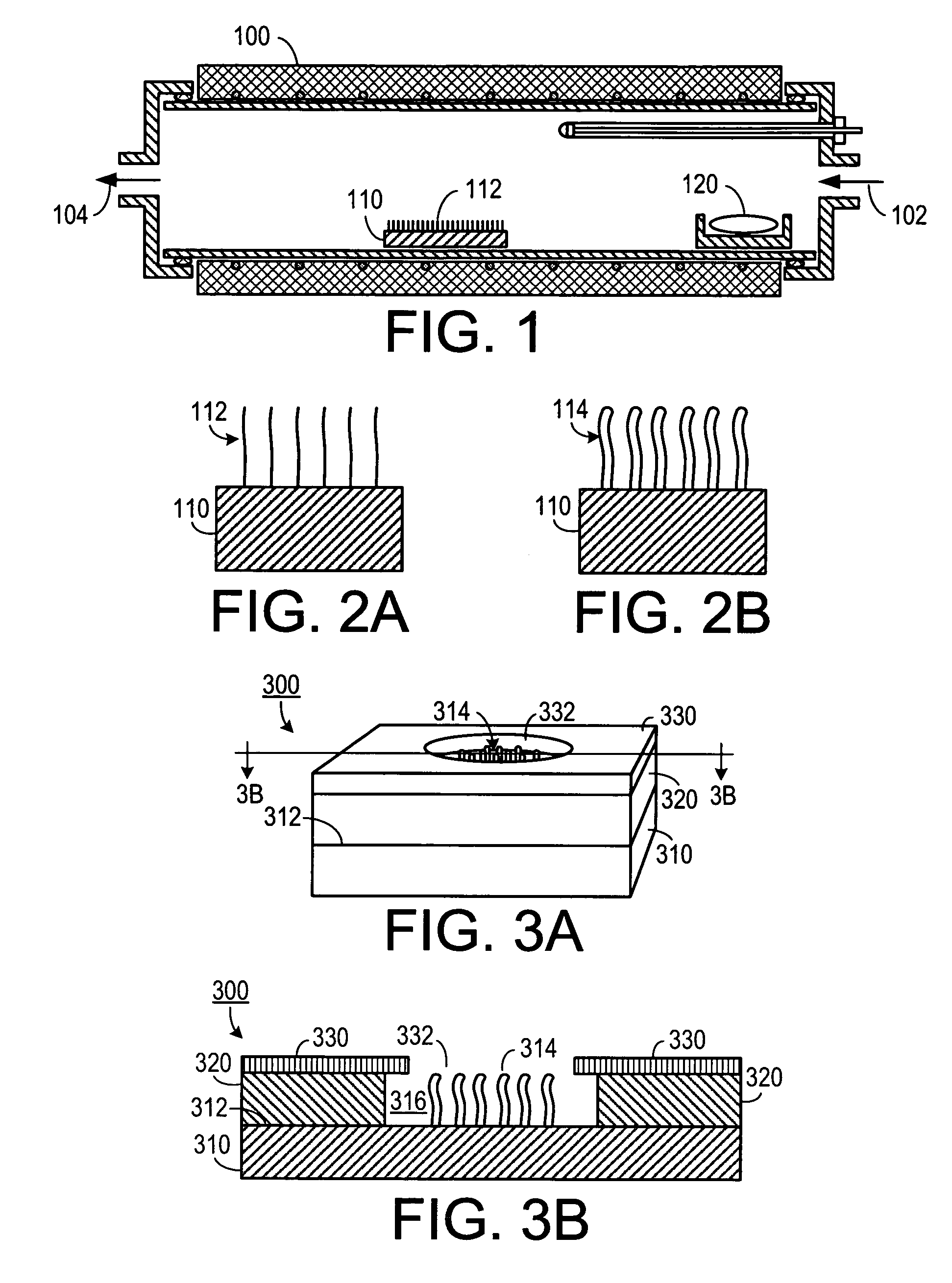
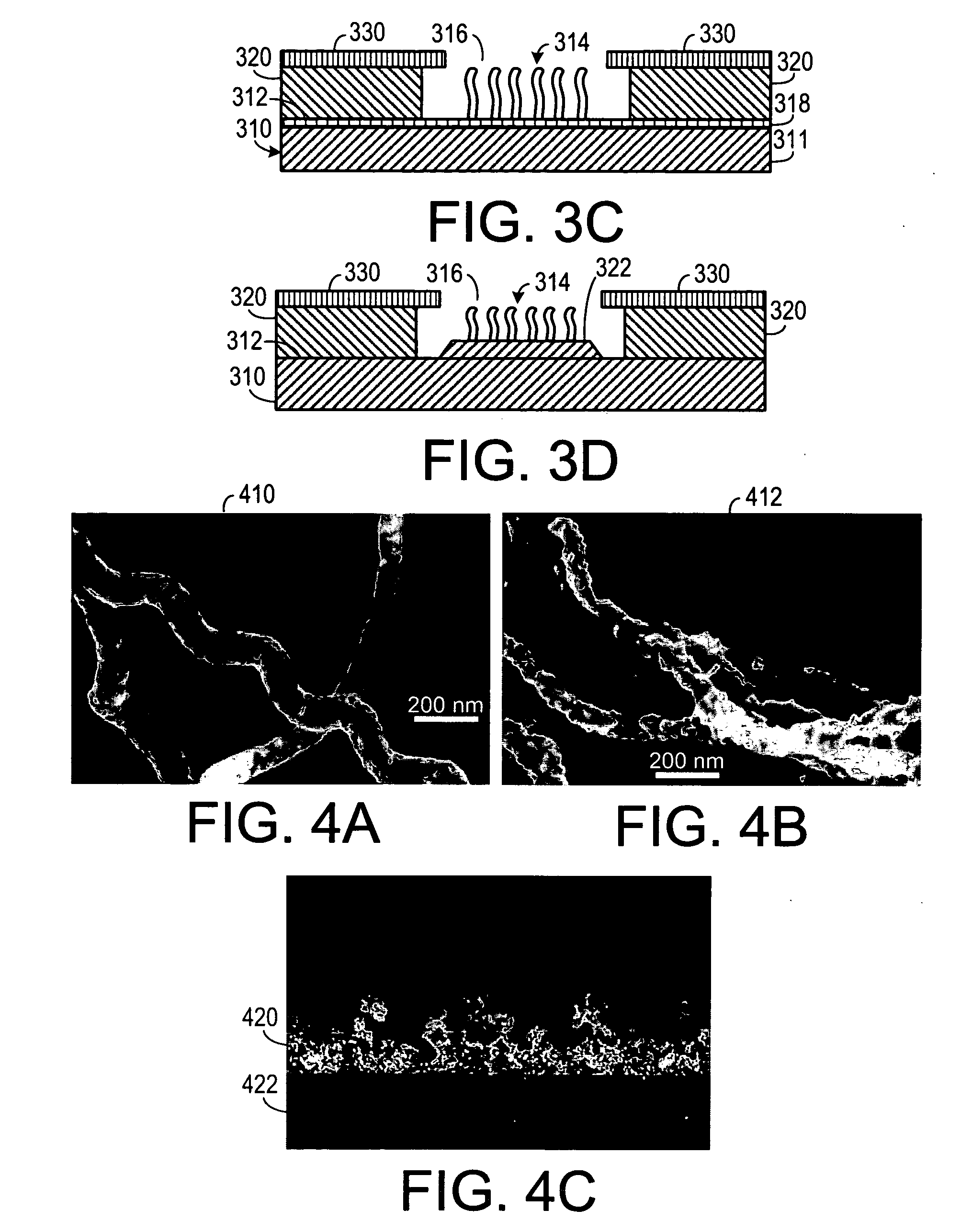
[0029] Also, as used herein, nanostructure means a structure having a narrowest dimension diameter of less than 800 nanometers (nm). as used herein, “metalized carbon nanostructures” include metal carbide nanostructures and metal carbide structures with carbon nanotube cores.

[0030] Metal carbide nanostructures are made as disclosed below. Such nanostructures may be used to form field emitting devices. Initially carbon nanotubes, either grown from a substrate through me...


PUM


Abstract

A structure includes a substrate and a metallized carbon nano-structure extending from a portion of the substrate. In a method of making a metallized carbon nanostructure, at least one carbon structure formed on a substrate is placed in a furnace. A metallic vapor is applied to the carbon nanostructure at a preselected temperature for a preselected period of time so that a metallized nanostructure

Description

FEDERALLY SPONSORED RESEARCH [0001] The United States Government may have certain rights in this invention pursuant to Cooperative Agreement No. 70NANB2H3030, awarded by the National Institute of Standards and Technology, United States Department of Commerce.BACKGROUND [0002] 1. Field of the Invention [0003] The invention relates to nano-scale structures and, more specifically, to a method of making nano-structures by carbon nanotube confined reactions. [0004] 2. Description of the Prior Art [0005] Field emission devices (gated or ungated) have applications in X-ray imaging systems, displays, electronics, microwave amplifiers, fluorescent lamp cathodes, gas discharge tubes, and many other electrical systems. Other applications for field emission devices include sensors, photonic bandgap devices, and wide bandgap semiconductor devices. [0006] Carbon nanotubes are currently being researched as electron emission sources in, for example, flat panel field emission display applications, m...

Claims


Application Information

Patent Timeline
IPC IPC(8): H01J1/02H01J1/38
CPCB82Y10/00H01J1/304H01J9/025H01J2201/30469
Inventor TSAKALAKOS, LOUCASHAN, SUNG SUOSAHENI, JOHN AIBANGBEEMANI, VANITA
Owner GENERAL ELECTRIC CO
Why Eureka
Try Eureka