Hard laminated film, method of manufacturing the same and film-forming device

a technology of laminated film and manufacturing method, which is applied in the direction of instruments, superimposed coating process, natural mineral layered products, etc., can solve the problems of difficult to precisely control the thickness of the thin film layer which is formed, difficult to adjust the film-forming rate, and difficult to manufacture samples having exactly the right particle size, etc., to achieve enhanced film-forming performance, high-efficiency gas ionization, and the effect of intensifying ion irradiation to the substra

Active Publication Date: 2005-08-04
KOBE STEEL LTD
View PDF12 Cites 112 Cited by
  • Summary
  • Abstract
  • Description
  • Claims
  • Application Information

AI Technical Summary

Benefits of technology

[0030] In the first aspect, as described above, the crystal particle size of the hard film A having a cubic rock-salt crystal structure as the main phase is simply, easily and finely controlled by adopting a laminated structure wherein two layers having mutually different crystal structures are combined together.
[0074] Further, in the aforesaid two variations of the sputter vaporization source according to the sixth aspect, a voltage is prevented from acting on the non-erosion area of the sputter vaporization source, so particles which have been sputtered from the erosion area react and combine with the reaction gas such as nitrogen in the non-erosion area and do not deposit. As a result, abnormal electrical discharge due to this factor is prevented, and high efficiency gas ionization takes place.

Problems solved by technology

However, it is extremely difficult to manufacture a sample having exactly the right particle size for a particular purpose, i.e., to manufacture a film having properties designed for a particular purpose, and there are practical problems involved.
For example, concerning the relative properties of an arc vaporization source and a sputter vaporization source, the arc vaporization source forms a film more rapidly than a sputter vaporization source, but it is difficult to adjust the film-forming rate, and difficult to precisely control the thickness of the thin film layer which is formed.
Even in a hard film having mainly a halide crystal structure, depending on the film-forming conditions, if the crystal particle size (hereafter, referred to also as crystal size) of the halide hard film is coarse, there is a limit to the improvement of wear resistance which can be obtained by increased hardness.
The film formed in this way does have increased hardness and improved wear resistance due to the finer crystal particles forming the film, but if the frictional coefficient of the film surface was not sufficiently reduced, there was little improvement of wear resistance and lubricity, and due to the increased hardness, the film was more liable to damage other members, hence, further improvement was desired.
Moreover, hard films formed by these prior art methods and techniques did not have sufficient performance to satisfy the increasingly stringent demands of cutting tools and sliding parts, so enhanced wear resistance and better durability were required.
It is thus very inconvenient to produce a sample having a specific particle size for a particular purpose, i.e., a film having properties designed for a particular purpose, and there is therefore a practical limit to the wear resistance enhancement of the hard film which can be obtained.
In the case of the aforesaid device, if an arc vaporization source and sputter vaporization source were operated in the same film-forming chamber, even if the arc vaporization source and sputter vaporization source were operated alternately, various problems could not be avoided, e.g., it was sometimes difficult to form a fine hard film or hard film having the desired composition depending on the hard film material and film-forming conditions, and abnormal electrical discharges sometimes occurred during the film-forming process.
Consequently, there was also a limit to the wear resistance enhancement which could be obtained by increasing the hardness of the film.
As a result, the concentration of discharged electrons becomes sparser, collisions with the sputter gas or reactive gas decrease, and it is difficult to perform high efficiency gas ionization.
Due to this insulator, there is a high probability of an abnormal discharge (arcing) occurring in the sputter vaporization source.
This also interferes with high efficiency gas ionization.
If there is interference with high efficiency gas ionization, ionic irradiation to the substrate cannot be intensified, so the fineness of the hard film layer cannot be increased, the surface becomes coarser and surface properties decline.
As a result, in the prior art film-forming device, and particularly when an arc vaporization source and sputter vaporization source were operated simultaneously in the same film-forming chamber, there was a serious limitation to the enhancement of properties and performance which can be achieved by increasing film hardness.

Method used


Image

  • Hard laminated film, method of manufacturing the same and film-forming device
  • Hard laminated film, method of manufacturing the same and film-forming device
  • Hard laminated film, method of manufacturing the same and film-forming device

Examples


first embodiment

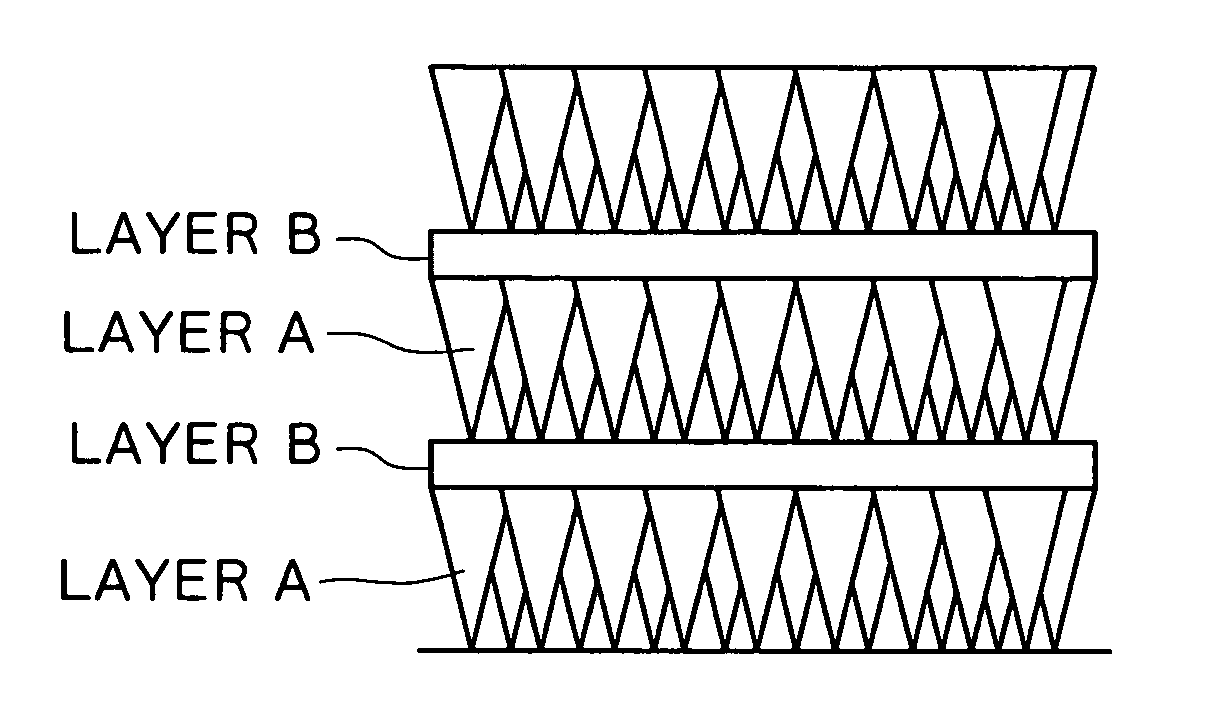
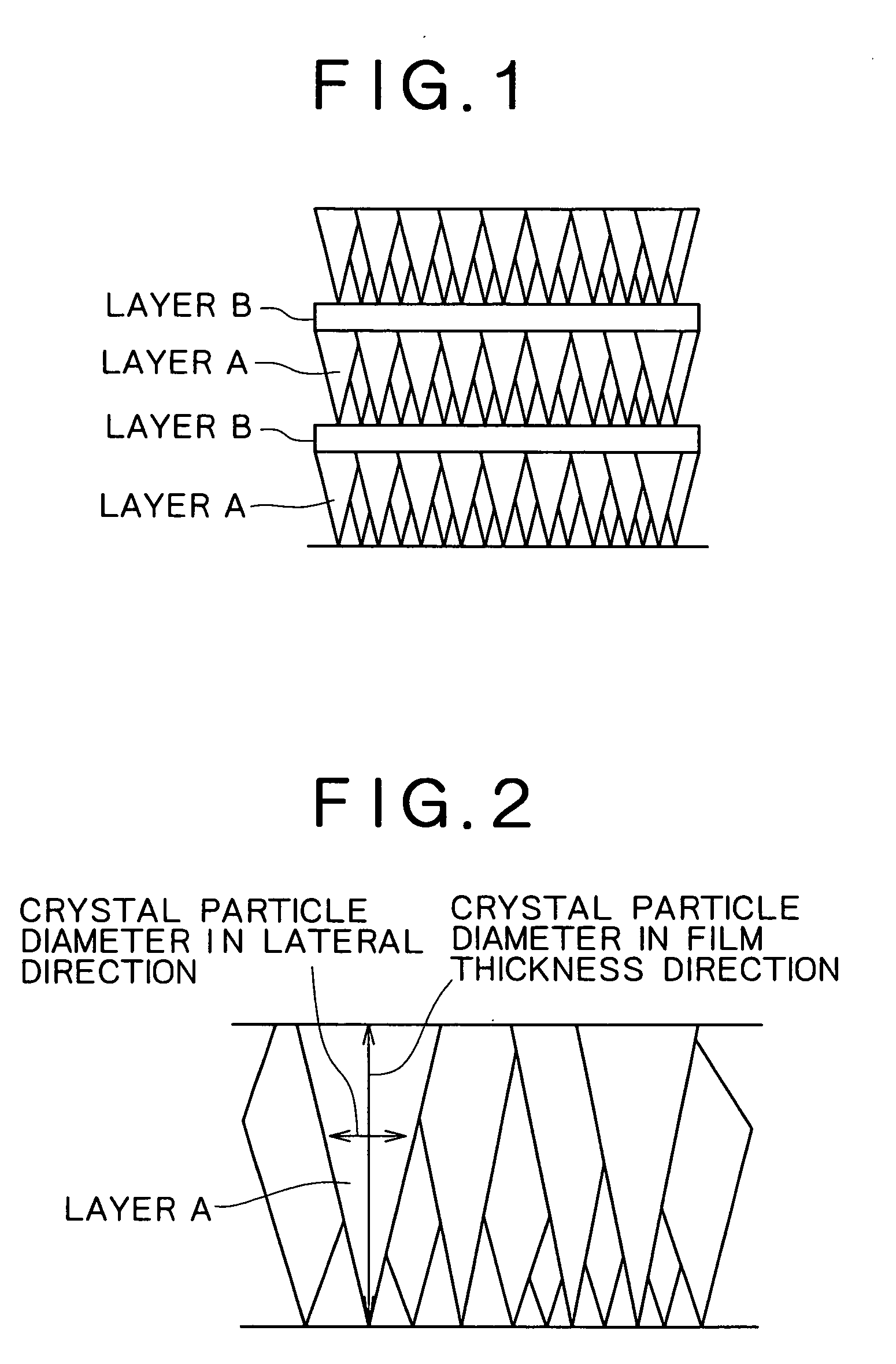
[0120] (Composition of Hard Film Layer A)

[0121] The composition formula of the hard film layer A which is the principal phase of the hard film of this invention, requires the selection of a substance having a rock-salt crystal structure, high hardness and wear resistance. This hard film having a rock-salt crystal structure may for example be a nitride, carbonitride or carbide having a cubic rock-salt structure containing Ti, Cr, Al or V such as TiN, CrN or TiAlN which are widely used in cutting tools and wear-resistant sliding parts. In addition, it may also be a compound of one or more elements selected from among 4A, 5A, 6A and Al or Si, with one or more elements selected from among B, C, N. These compounds all have a cubic rock-salt structure, high hardness and superior wear resistance. If a minute amount of 10% or less (0.1 or less in terms of atomic ratio) of oxygen is added to layer A within a range in which the rock-salt crystal structure of the hard film layer A is maintain...

second embodiment

[0128] The Inventors discovered that, by forming the layer A having a chemical composition corresponding to the following formula (1) and the layer B having a chemical composition corresponding to the following formula (2) so that the aforesaid deposition requirements are satisfied, a hard film having superior wear resistance and lubricity was obtained, and thereby arrived at the present invention. [0129] Layer A: Cr (BaCbN1-a-b-cOc)e

0≦a≦0.15, 0≦b≦0.3, 0≦c≦0.1, 0.2≦e≦1.1  (1) [0130] Layer B: B1-x-tCsNt

0≦s≦0.25, (1−s−t) / t≦1.5  (2)

[0131] The reason for specifying the composition of Layer A and Layer B as mentioned above, will now be described in detail.

[0132] [Composition of Layer A]

[0133] First, the reason why layer A is a Cr (B, C, N, O) film containing B, C, N, O in the proportions shown in the aforesaid formula (1), is as follows.

[0134] Layer A has chromium nitride (CrN, Cr2N) of high hardness as its main component so that the film retains its wear resistance. The hardness ca...

third embodiment

[0154] (Composition of Layer A)

[0155] The composition of layer A, which is the main phase of the hard laminated film according to the third embodiment, should have high oxidizing properties in applications wherein sliding parts such as cutting tools reach a high temperature. The layer A must also have the basic properties required of the hard film, such as high hardness and wear resistance.

[0156] For this reason, the composition of layer A may be represented by:

[0157] Formula 1: (Ti1-x-yAlxMy)(BaCbN1-a-b-cOc) [wherein, x, y, a, b, c are respectively atomic ratios, 0.4≦x≦0.8, 0≦y≦0.6, 0≦a≦0.15, 0≦b≦0.3, 0≦c≦0.1, and M is one or metal elements selected from among 4A, 5A, 6A, Si.

[0158] Among the compositions of layer A represented by Formula 1, (Ti1-x-yAlxMy)(BaCbN1-a-b-cOc) [wherein x, y, a, b, c are respectively atomic ratios 0.5≦x≦0.8, 0.05≦y≦0.6, 0≦a≦0.15, 0≦b≦0.3, 0≦c≦0.1, and M is one or metal elements selected from among Cr, V, Si], is preferred.

[0159] In the aforesaid Form...


PUM

PropertyMeasurementUnit
thicknessaaaaaaaaaa
thicknessaaaaaaaaaa
θ-aaaaaaaaaa

Abstract

A hard laminated film wherein a layer A and a layer B having specific compositions are deposited alternately so that the compositions of layer A and layer B are different. The thickness of layer A per layer is twice or more the thickness of layer B per layer, the thickness of layer B per layer is 0.5 nm or more, and the thickness of layer A per layer is 200 nm or less. Layer A has a cubic rock-salt crystal structure such as that of Ti, Cr, Al, V nitride, carbonitride or carbide, and layer B is a hard film having a crystal structure other than cubic such as that of BN, BCN, SiN, SiC, SiCN, B—C, Cu, CuN, CuCN or metallic Cu. Alternatively, layer A has a chemical composition satisfying the following formula (1), and layer B has a chemical composition satisfying the following formula (2). Layer A: Cr(BaCbN1-a-b-cOc) 0≦a≦0.15, 0≦b≦0.3, 0≦c≦0.1, 0.2≦e≦1.1  (1) Layer B: B1-s-tCsNt 0≦s 0.25, (1−s−t) / t≦1.5  (2) Alternatively, Layer A has a specific atomic ratio composition of (Ti1-x-yAlxMy)(BaCbN1-a-b-cOc) and Layer B has one or more specific atomic ratio compositions selected from among the compositions B1-x-yCxNy, Si1-x-yCxNy, C1-xNx, Cu1-y(CxN1-x)y. Alternatively, Layer A has one of the following Compositional Formulae 1 or 2. Formula 1: (Ti1-x-yAlxMy), (BaCbN1-a-b-cOc), Formula 2: (Cr1-αXα)(BaCbN1-a-b-cOc)e (X is one or more metal elements selected from among Ti, Zr, Hf, V, Nb, Ta, Mo, W, Al, Si. Layer B has the following compositional formula 3. Formula 3 M(BaCbN1-a-b-cOc). M is one or more metal elements selected from among W, Mo, V, Nb.

Description

BACKGROUND OF THE INVENTION [0001] This invention relates to a hard laminated film whereof the crystal particle size is finely controlled having superior mechanical resistance, to a hard laminated film having wear resistance formed on the surface of machining tools or sliding parts for automobiles, and to a hard laminated film having superior wear resistance and anti-oxidation properties. [0002] This invention further relates to a composite film-forming device comprising an arc vaporization source and a sputter vaporization source which can form this hard laminated film having superior properties. [0003] In recent years, there has been an increasing need to improve the wear resistance of super hard alloys, cutting tools having thermit or high-speed tool steel as base materials and sliding parts for automobiles, and the possibility of improving the wear resistant film used on the surface of these parts is being considered. [0004] The wear resistant film used in the prior art comprise...

Claims


Application Information

Patent Timeline
Patent Type & Authority Applications(United States)
IPC IPC(8): B32B9/00C23C14/00C23C14/06C23C14/16C23C14/22C23C14/24C23C14/32C23C14/34C23C14/35C23C14/54C23C14/56C23C28/00C23C30/00
CPCC23C14/0036Y10T428/24942C23C14/06C23C14/0641C23C14/0647C23C14/0652C23C14/0664C23C14/0676C23C14/16C23C14/22C23C14/325C23C14/35C23C14/568C23C28/044C23C28/322C23C28/34C23C28/347C23C28/42C23C28/44C23C30/00C23C28/341Y10T428/26Y10T428/24975C23C14/0063C23C28/00C23C14/00
Inventor YAMAMOTO, KENJIKUJIME, SUSUMUTAKAHARA, KAZUKIFUJII, HIROFUMI
Owner KOBE STEEL LTD
Why Eureka
Try Eureka