Pixel circuit substrate, liquid crystal display apparatus, method of manufacturing the same and projection display apparatus

a liquid crystal display and substrate technology, applied in non-linear optics, instruments, optics, etc., can solve the problems of capacitor leakage, inability to ensure the necessary capacitance value, and detrimental effect of decreasing contrast, and achieve high brightness, large image contrast, and low cost

Inactive Publication Date: 2006-05-11
VISTA PEAK VENTURES LLC
View PDF2 Cites 19 Cited by
  • Summary
  • Abstract
  • Description
  • Claims
  • Application Information

AI Technical Summary

Benefits of technology

[0014] The present invention has been made in view of the problems as described above and has its object the provision of a liquid crystal display apparatus which has high brightness and large image contrast and can be manufactured at low cost and with ease, a method of manufacturing this liquid crystal display apparatus, and a projection display apparatus.

Problems solved by technology

However, it becomes impossible to ensure necessary capacitance values if storage capacitors are too much miniaturized.
However, when the manufacturing method described in reference 1 above is actually performed, it has been proven experimentally that such approach results in capacitor leakage.
This has the detrimental effect of decreasing contrast.
As a result of such nonuniformity, leakage current is generated in those portions where the spacing between the two electrodes narrows.
However, the above-described conventional techniques have the following problems.
For this reason, only an insulating film formed at a low temperature can be used as the capacitor insulating film of the storage capacitor, with the result that only a capacitor of low insulating properties can be used.

Method used


Image

  • Pixel circuit substrate, liquid crystal display apparatus, method of manufacturing the same and projection display apparatus
  • Pixel circuit substrate, liquid crystal display apparatus, method of manufacturing the same and projection display apparatus
  • Pixel circuit substrate, liquid crystal display apparatus, method of manufacturing the same and projection display apparatus

Examples


first embodiment

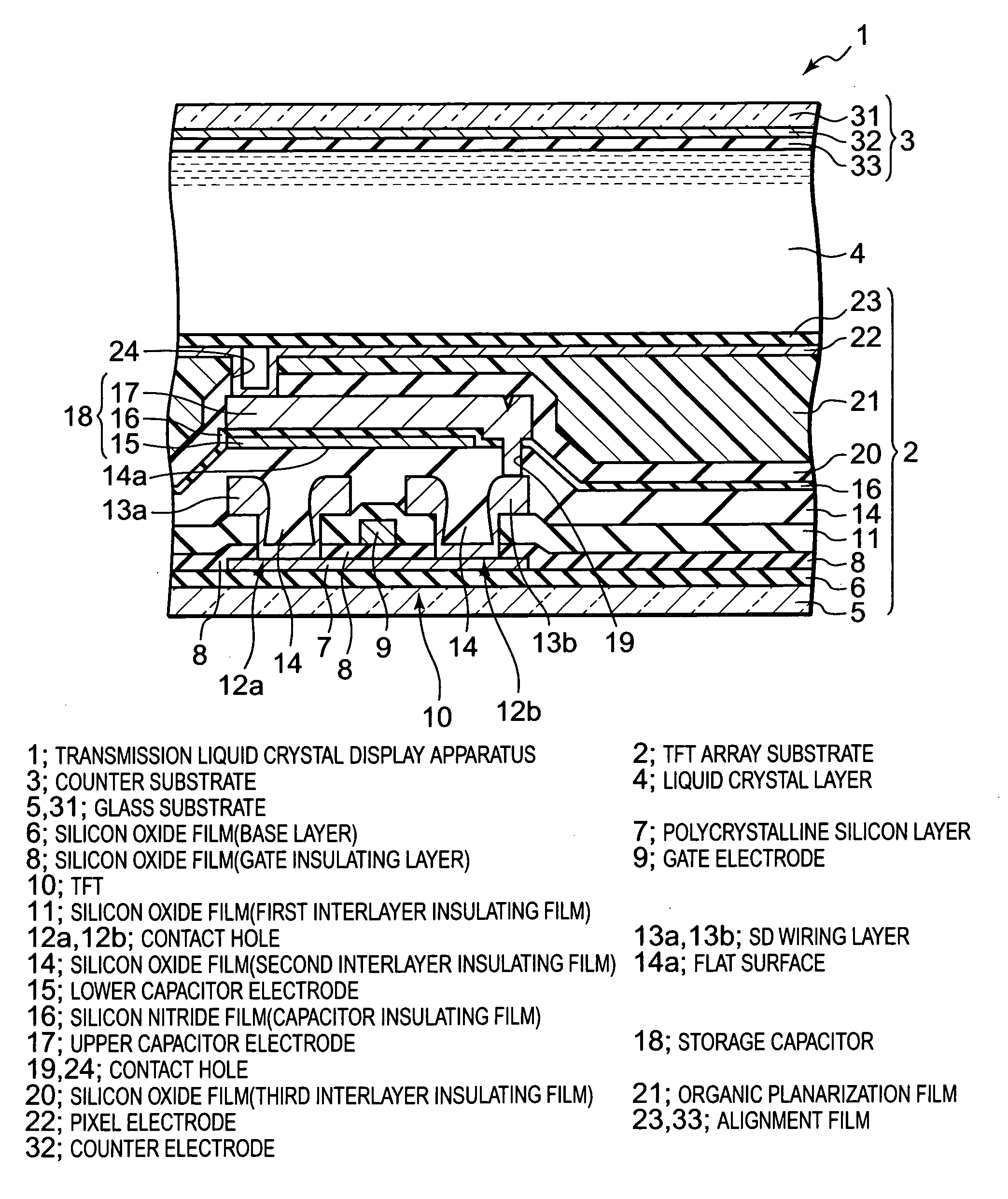
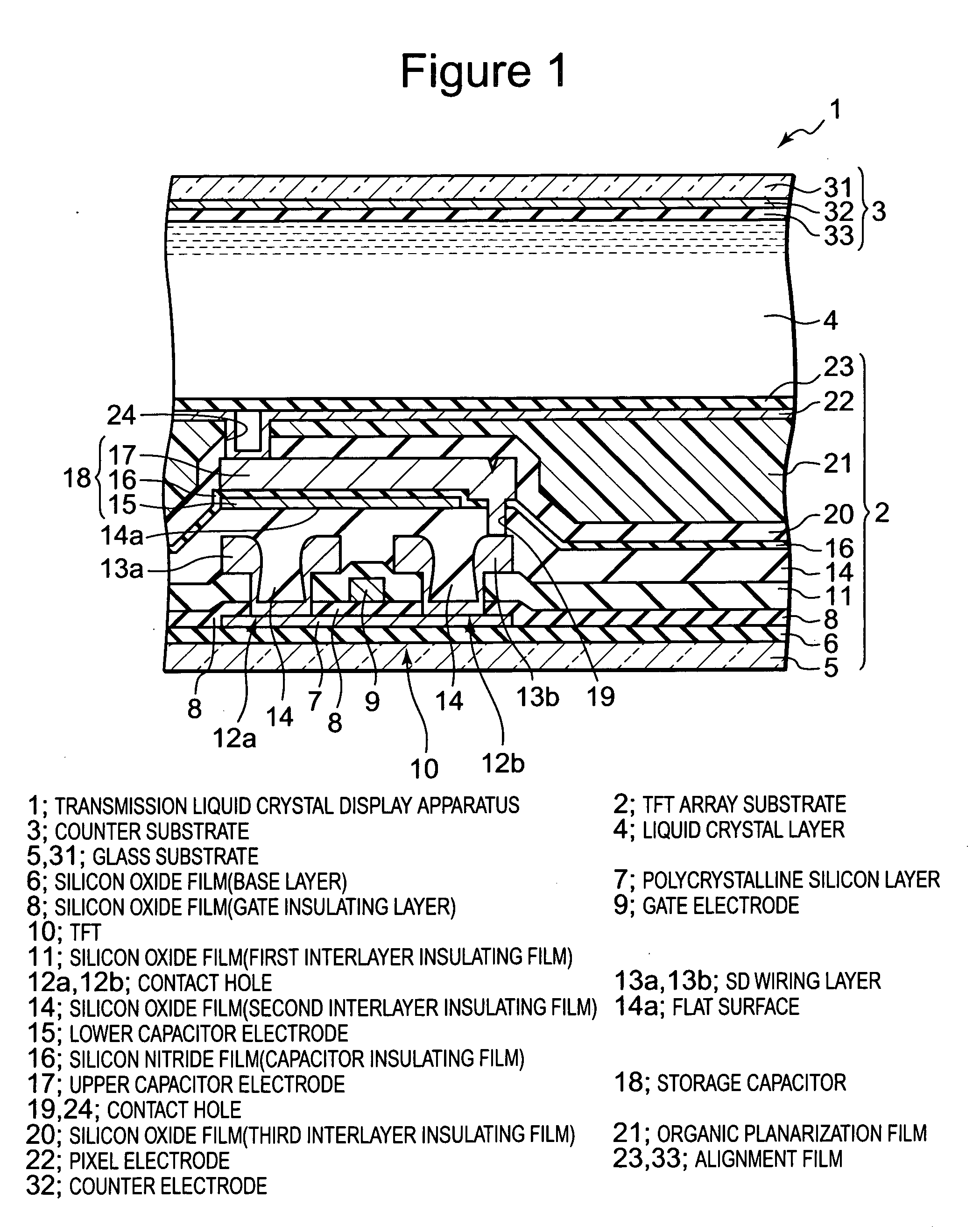
[0069] And the TFT array substrate 2 and the counter substrate 3 are bonded together via a spacer (not shown) in such a manner that the alignment film 23 and the alignment film 33 are opposed to each other. Next, a liquid crystal is implanted between the TFT array substrate 2 and the counter substrate 3, whereby a liquid crystal layer 4 is formed. As a result of this, a transmission type liquid crystal display apparatus 1 is manufactured. The advantages of this embodiment are the same as in the above-described

[0070] Incidentally, in the above-described first and second, embodiments, an example in which in the step shown in FIG. 6 A, the upper layer of the silicon oxide film 14 (second interlayer insulating film) is formed from a high concentration O3-TEOS-based SiO2 film was shown. However, the present invention is not limited to this, and the upper layer of the silicon oxide film 14 may be formed from an SiO2 film formed by an O3-HMDSO (hexamethyldisiloxane) reaction by a normal pr...

fourth embodiment

[0080] Next, the present invention will be described. FIG. 11 is a drawing which shows a liquid crystal projector as a projector apparatus related to this embodiment. A liquid crystal display apparatus related to this embodiment is, for example, a front projection type projector. However, this maybe a front projection type home projector or a rear projection type home projector.

[0081] As shown in FIG. 11, in a liquid crystal projector apparatus 80 related to this embodiment, a halogen lamp 81 which emits white light is provided as a light source. A half mirror 82a which transmits red light and reflects green light and blue light is provided in a position which is irradiated with the white light emitted from the halogen lamp 81, and a mirror 83a is provided in a position which is irradiated with the red light transmitted through the half mirror 82a. Furthermore, a half mirror 82b which transmits blue light and reflects green light is provided in a position which is irradiated with th...

third embodiment

[0082] A light bulb for red color 84R is provided in such a manner as to lie in the light path of red light reflected by the mirror 83a, a light bulb for green color 84G is provided in such a manner as to lie in the light path of green light reflected by the half mirror 82b, and a light bulb for blue color 84B is provided in such a manner as to lie in the light path of blue light reflected by the mirror 83c. The light bulb for red color 84R, the light bulb for green color 84G and the light bulb for blue color 84B are each a monochromatic liquid crystal display apparatus and is a transmission type liquid crystal display apparatus related to the above-described first or

[0083] Furthermore, in a position on which the light transmitted through the light bulb for red color 84R, the light transmitted through the light bulb for green color 84G and the light transmitted through the light bulb for blue color 84B become incident, there is provided prism 85 which synthesizes these three kinds o...


PUM

PropertyMeasurementUnit
concentrationaaaaaaaaaa
thicknessaaaaaaaaaa

Abstract

A pixel circuit substrate includes a first interlayer insulating film which is made of an inorganic material at least in a source and drain regions of a thin film transistor. A contact hole is formed in an area above the source and drain regions of a thin film transistor in the first interlayer insulating film. A wiring layer is formed on the first interlayer insulating film, extends to an inner wall and a bottom surface of the contact hole. On a top surface of the wiring layer is formed a recess reflecting the shape of a contact hole. A second interlayer insulating film is formed on the wiring layer, embedded in the recess and has a flat top surface in an area above the thin film transistor. A storage capacitor on the second interlayer insulating film is disposed in the area above the thin film transistor.

Description

BACKGROUND OF THE INVENTION [0001] 1. Field of the Invention [0002] The present invention relates to a liquid crystal display apparatus in which a thin film transistor and a storage capacitor are provided in each pixel, a method of manufacturing this liquid crystal display apparatus, and a projection display apparatus which uses the liquid crystal display apparatus as a light bulb. [0003] 2. Description of Related Art [0004] Electrooptic apparatus, such as liquid crystal display apparatus, are used as direct-view display units of various kinds of equipment, and they are also used in light bulbs of projection display apparatus, such as a data projector. Among these electrooptic apparatus, in an active matrix type liquid crystal display apparatus, a TFT array substrate and a counter substrate which is disposed opposite to this TFT array substrate are provided, and a liquid crystal as an electrooptic substance is disposed between the two substrates. In the TFT array substrate, multiple...

Claims


Application Information

Patent Timeline
Patent Type & Authority Applications(United States)
IPC IPC(8): G02F1/136
CPCG02F1/136213G02F1/136227
Inventor SHIOTA, KUNIHIROTANABE, HIROSHI
Owner VISTA PEAK VENTURES LLC
Why Eureka
Try Eureka