Method for etching chromium thin film and method for producing photomask

a technology of chromium-based thin film and dry etching, which is applied in the direction of originals for photomechanical treatment, instruments, optics, etc., can solve the problems of size and shape, the inability to meet the demand for a higher-resolution pattern of photomask following the development of a higher degree of integration of semiconductor integrated circuits, and the obstacle to practical us

Active Publication Date: 2006-05-18
HOYA CORP
View PDF16 Cites 160 Cited by
  • Summary
  • Abstract
  • Description
  • Claims
  • Application Information

AI Technical Summary

Benefits of technology

[0064] The method of manufacturing a photomask according to the eighteenth or the nineteenth aspect, wherein, by etching the light-shielding film, a pattern including a pattern of which a design size is 0.4 μm or more and 2.0 μm or less and of which a CD linearity error is 15 nm or less is formed.

Problems solved by technology

However, such a demand for a higher-resolution pattern of the photomask following the development of a higher degree of integration of the semiconductor integrated circuit can not be met by an existing patterning method of patterning a chromium-based light-shielding film using a resist pattern as an etching mask.
It has been revealed that, in this method, as a fine opening pattern (hole) has a higher resolution, an influence of degradation in size and shape of the fine opening pattern (hole) due to a microloading effect can not be neglected and becomes an obstacle in practical use.
However, in recent years, a pattern having a fine and complicated shape, such as an optical proximity correction (OPC) pattern, is used.
Under the circumstances, it is difficult to form a high-accuracy pattern by using the existing method.
This results in differences in size and in corner shape between these patterns.
First, the corners of the square opening pattern being rounded induces occurrence of a suspected defect, resulting in a serious obstacle to an inspection process.
Further, the pattern shape is not formed in exact conformity with designed pattern data, resulting in reduction in margin in a lithography process in a semiconductor manufacturing process and a large number of steps required in condition setting.
Further, the above-mentioned conversion difference becomes an obstacle to fine pattern formation on the mask.
In this case, however, the sizing amount increases so that a conversion time increases.
As a second problem, because of the microloading effect, the conversion difference between the resist and Cr widely changes depending on the size of the opening pattern (hole).
At first, because of this problem, the conversion difference varies depending on the size of the opening pattern so that CD accuracy (particularly, the CD linearity) is degraded.
This results in reduction in margin in the lithography process in the semiconductor manufacturing process and a large number of steps required in condition setting.
Although the CD accuracy may be compensated by another process such as exposure, a condition therefor may not be an optimal condition considering other CD accuracy than the CD linearity.
This results in reduction in margin in the lithography process in the semiconductor manufacturing process and a large number of steps required in condition setting.
Further, in case where the length of the mask is measured by an optical length meter, length measurement accuracy is degraded.

Method used


Image

  • Method for etching chromium thin film and method for producing photomask
  • Method for etching chromium thin film and method for producing photomask
  • Method for etching chromium thin film and method for producing photomask

Examples


first embodiment

[0072] In a first embodiment of the present invention, upon etching a chromium-based thin film made of a material containing chromium by the use of a resist pattern as a mask, etching is carried out by the use of a chemical species produced by preparing a dry etching gas comprising a mixed gas containing a halogen-containing gas and an oxygen-containing gas and supplying a plasma excitation power to the dry etching gas to thereby excite plasma. As the plasma excitation power, a power lower than a plasma excitation power at which plasma density jump occurs is used.

[0073] For example, in case of the ICP system, the plasma excitation power is ICP power. As regards the plasma density jump, the above-mentioned second prior art describes the relationship between a plasma electron density and the ICP power. When the ICP power increases, the plasma electron density tends to increase and, at a certain ICP power, density jump occurs as a phenomenon that the plasma electron density rapidly in...

second embodiment

[0086] In a second embodiment of the present invention, upon etching a chromium-based thin film made of a material containing chromium by the use of a resist pattern as a mask, etching is carried out by the use of a chemical species produced by preparing a dry etching gas comprising a mixed gas containing chlorine and oxygen and supplying a plasma excitation power to the dry etching gas to thereby excite plasma. The thin film is etched in presence of an organic substance other than the resist pattern while supplying at least a part of the chemical species to the thin film in a direction perpendicular to the thin film. Thus, the etching is carried out while depositing an organic product on a side wall of a resist layer etched by an isotropic etching component.

[0087] According to the second embodiment of the present invention, the dry etching is performed in presence of the organic substance other than the resist pattern while supplying at least a part of the chemical species to the ...

example 1

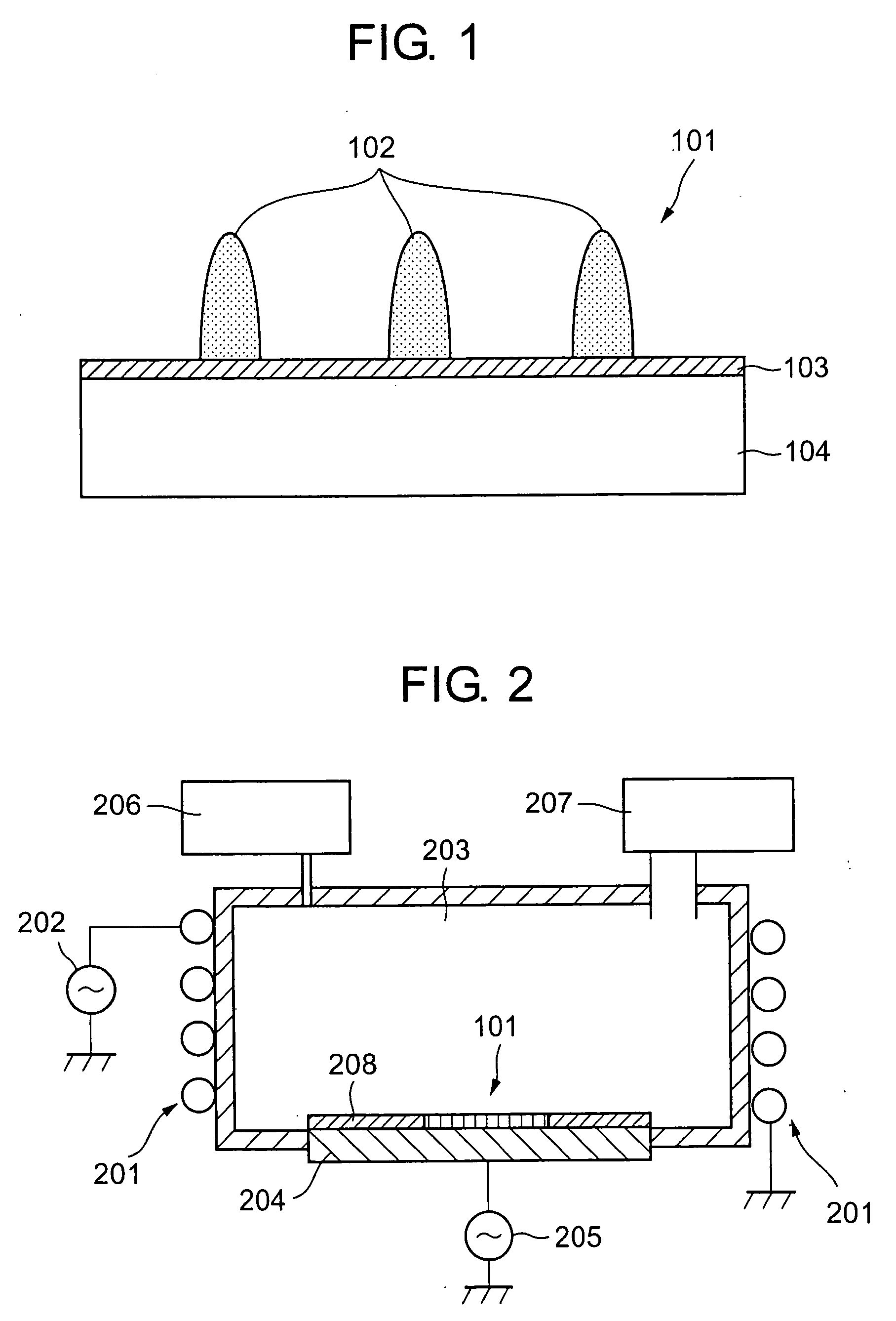
[0100] First, FIG. 1 shows a mask substrate 101 provided with a resist pattern, which is an object of etching in this example. The mask substrate 101 has a layered structure comprising a resist pattern 102 having a thickness of 400 nm, a Cr-based film (representing a film made of a material containing Cr; the same also applies hereinafter) 103 having a thickness of 100 nm, and a glass substrate (synthetic quartz substrate or the like) 104. As the resist pattern 102, a photoresist or an EB resist is used depending on an exposure apparatus to be used. In either case, each side wall of the resist pattern is approximately vertical in section. The resist pattern 102 covers 80% or more of an area of the Cr-based film 103.

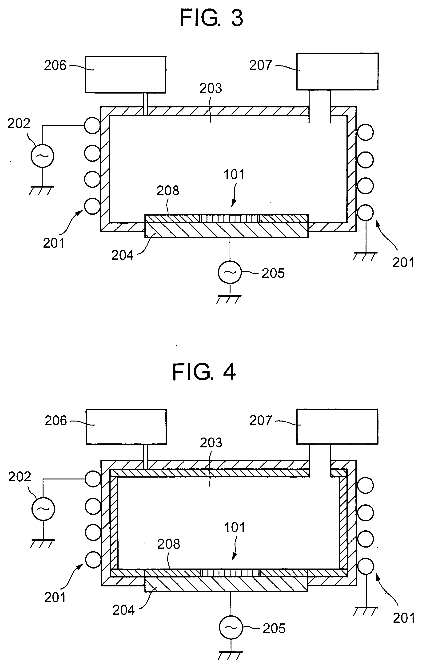
[0101] Next, FIG. 2 shows a structure of an etching apparatus (of an inductive coupling plasma (ICP) system) used in this example.

[0102] This apparatus comprises a plasma generation coil 201, a coil-energizing RF power supply 202, a vacuum chamber (hereinafter referred ...


PUM

PropertyMeasurementUnit
sizeaaaaaaaaaa
sizeaaaaaaaaaa
sizeaaaaaaaaaa

Abstract

An object to be processed has a chromium-based thin film made of a material containing chromium. The thin film is etched using a resist pattern as a mask. The thin film is etched by the use of a chemical species produced by preparing a dry etching gas containing a halogen-containing gas and an oxygen-containing gas and supplying a plasma excitation power to the dry etching gas to thereby excite plasma. The thin film is etched using, as the plasma excitation power, a power lower than a plasma excitation power at which plasma density jump occurs.

Description

TECHNICAL FIELD [0001] The present invention relates to a method of dry etching a chromium-based thin film and, in particular, to a method of dry etching a light-shielding film comprising a chromium-based thin film, which method is carried out in a method of manufacturing a photomask used in semiconductor device manufacturing or the like. Further, the present invention relates to a method of manufacturing a photomask, which method includes a step of dry etching a light-shielding film comprising a chromium-based thin film. BACKGROUND ART [0002] For example, following development of a higher degree of integration of a semiconductor integrated circuit or the like, a photomask used in a micromachining process contained in a semiconductor manufacturing process is required to have a high pattern accuracy. [0003] In photomasks currently used, a chromium-based material is generally used as a light-shielding film in view of machinability of a high-accuracy pattern. [0004] However, such a dem...

Claims


Application Information

Patent Timeline
Patent Type & Authority Applications(United States)
IPC IPC(8): C23F1/00C23F4/00G03F1/36G03F1/68G03F1/80
CPCC23F4/00G03F1/80G03F1/54H01L21/3065
Inventor KIMURA, YASUKI
Owner HOYA CORP
Why Eureka
Try Eureka