Methods for dicing a released CMOS-MEMS multi-project wafer

a technology of cmosmems and multi-project wafers, applied in the field of dicing processes, can solve the problems of damage to released micromachined devices, limited use of micromachined structures, and lack of protective layers, and achieve the effect of high reliability

Inactive Publication Date: 2006-05-18
NAT APPLIED RES LAB NAT CHIP IMPLEMENTATION CENT
View PDF10 Cites 14 Cited by
  • Summary
  • Abstract
  • Description
  • Claims
  • Application Information

AI Technical Summary

Benefits of technology

[0009] Because of their simplicity and high reliability, these two methods are expected to benefit t

Problems solved by technology

However, unlike the standard integrated circuit (IC) package where the circuits have rigid passivation, micromachined structures are restricted to the movable architecture and the absence of protective layer.
For this reason, one of the main challenges in fabricating CMOS-MEMS multi-project wafers is to protect the released microstructures during dicing the wafers.
Conventional dicing machine uses water to cool the rotating

Method used


Image

  • Methods for dicing a released CMOS-MEMS multi-project wafer
  • Methods for dicing a released CMOS-MEMS multi-project wafer
  • Methods for dicing a released CMOS-MEMS multi-project wafer

Examples


Embodiment Construction

[0024] Two reliable methods are proposed to overcome the destruction and damage issues.

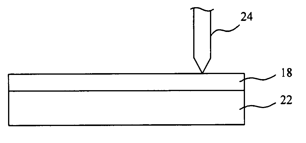
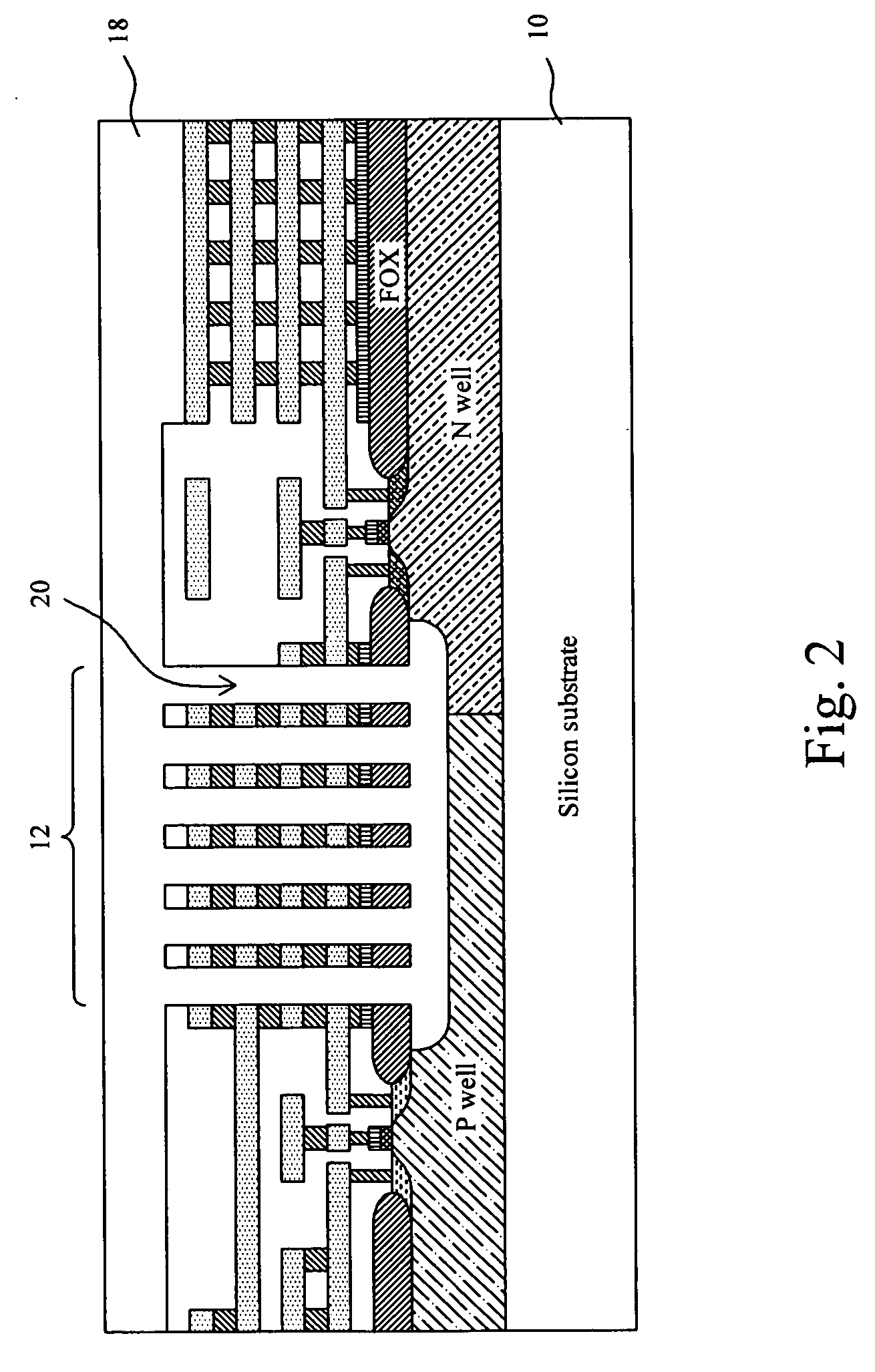
[0025] In this method, as shown in FIG. 2, a thick photoresist 18 is used to protect the released microstructure 12, in which the photoresist 18 fills into the gaps 20 in the released microstructure 12 and covers over the released microstructure 12. FIG. 3 is an illustrative diagram when dicing a released CMOS-MEMS multi-project wafer by this method, in which the wafer 22 includes released structures, e.g. the microstructure 12 as shown in FIG. 2, and the photoresist 18 is spun on the full wafer surface to cover all cavities and structures on the wafer 22. The photoresist 18 is used to protect the released structures on the wafer 22 during the dicing process with a diamond blade 24. Further detail steps are illustrated by a flowchart shown in FIG. 4. After the microstructures on the wafer 22 are released by post processes 26, in step 28 the photoresist 18, of about 15 μm for example, is spun on t...


PUM


Abstract

Simple but practical methods to dice a CMOS-MEMS multi-project wafer are proposed. On this wafer, micromachined microstructures have been fabricated and released. In a method, a photoresist is spun on the full wafer surface, and this photoresist is thick enough to cover all cavities and structures on the wafer, such that the photoresist will protect the released structures free from the chipping, vibrations, and damages in the diamond blade dicing process. In another method, a laser dicing system is utilized to scribe the multi-project wafer placed on a platform, and by precisely controlling the platform moving-track, the dicing path can be programmed to any required shape and region, even it is not straight. In addition, the wafer backside is mounted on a blue-tape at the beginning to enhance the process reliability.

Description

REFERENCE TO RELATED APPLICATIONS [0001] This Patent Application is based upon Provisional Patent Application Ser. 60 / 626,925 filed on 12 Nov. 2004.FIELD OF THE INVENTION [0002] The present invention is generally related to wafer dicing processes and, more particularly, to methods for dicing a released CMOS-MEMS multi-project wafer. BACKGROUND OF THE INVENTION [0003] There are many advantages to leverage the complementary metal-oxide-semiconductor (CMOS) process for microelectromechanical systems (MEMS). For passive radio frequency (RF) components, such as high-quality (high-Q) inductors using bulk micromachining to remove the silicon substrate enable to eliminate the substrate losses, parasitic effects and coupling interference, so that their self-resonant frequency and quality factor can be improved. Other micromachining devices, such as high-Q mechanical resonators, filters, RF low loss switches, tunable capacitors, and some representative components have also been designed and v...

Claims


Application Information

Patent Timeline
IPC IPC(8): H01L21/78
CPCB81C1/00896B81C2201/053
Inventor TSENG, SHENG-HSIANGXIAO, FU-YUANJUANG, YING-ZONGCHIU, CHIN-FONG
Owner NAT APPLIED RES LAB NAT CHIP IMPLEMENTATION CENT
Why Eureka
Try Eureka