Ultraviolet assisted pore sealing of porous low k dielectric films

a low-k dielectric film, ultra-violet technology, applied in the direction of coatings, metallic material coating processes, chemical vapor deposition coatings, etc., can solve the problems of affecting the dielectric constant, affecting the integration of porous low-k materials in the manufacture of semiconductor devices, and in general difficult to achiev

Inactive Publication Date: 2006-05-18
AXCELIS TECHNOLOGIES
View PDF12 Cites 396 Cited by
  • Summary
  • Abstract
  • Description
  • Claims
  • Application Information

AI Technical Summary

Problems solved by technology

However, the integration of porous low-k materials in the manufacture of the semiconductor device, in general, has proven difficult.
For example, because of the open nature of the porous low k dielectric materials, process gases and chemistries employed in subsequent processing (i.e., after formation of the porous low k dielectric material)) may diffuse into the porous network where they become trapped where they can cause damage as well as alter the dielectric constant.

Method used


Image

  • Ultraviolet assisted pore sealing of porous low k dielectric films
  • Ultraviolet assisted pore sealing of porous low k dielectric films

Examples


example 1

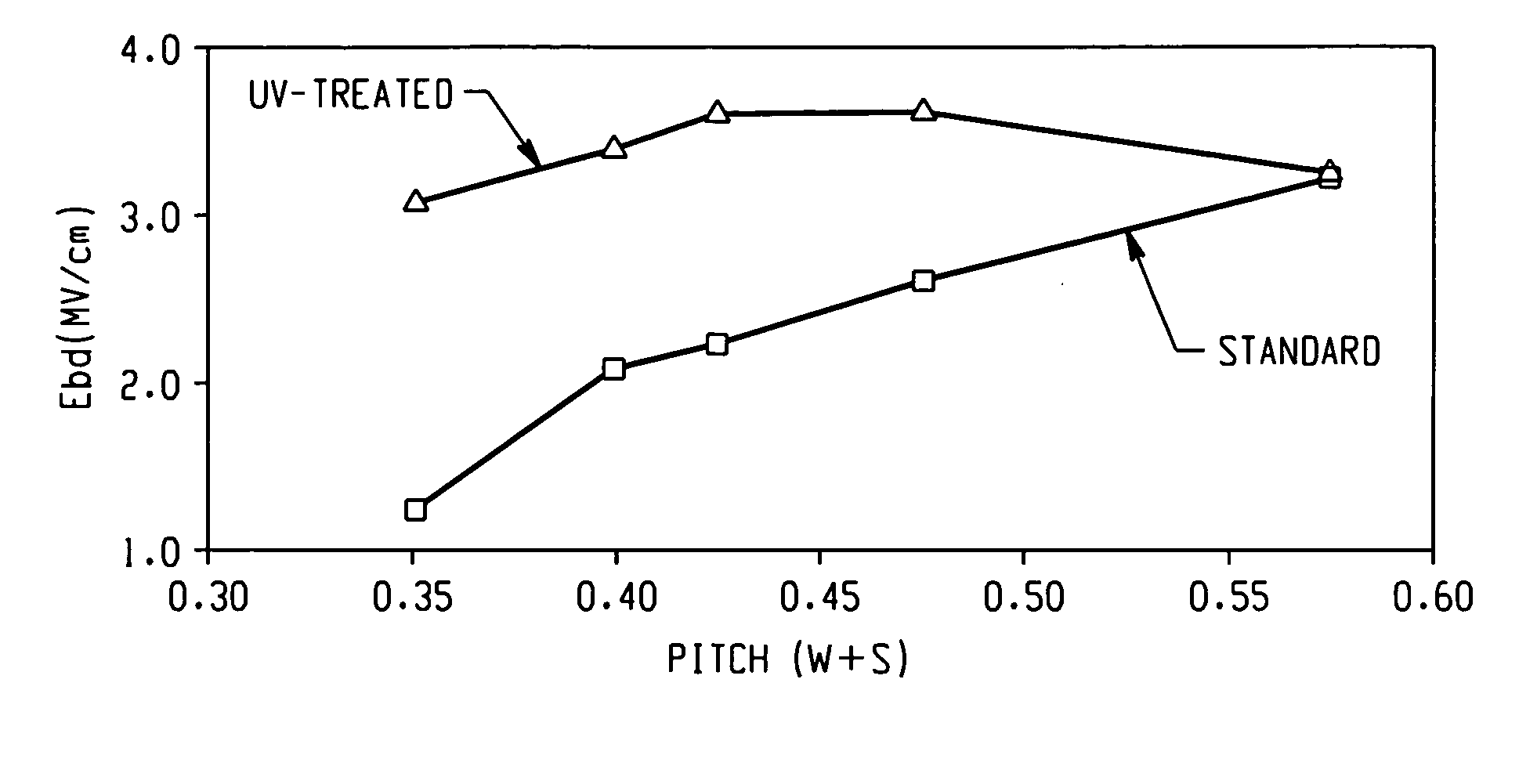
[0042] In this Example, breakdown voltage as a function of pitch was measured before and after UV sealing the patterned porous dielectric material in accordance with the present disclosure. Both substrates were annealed. The line width was 175 microns. As shown in the FIG. 1, a significant improvement in the breakdown field was observed for the dense array.

example 2

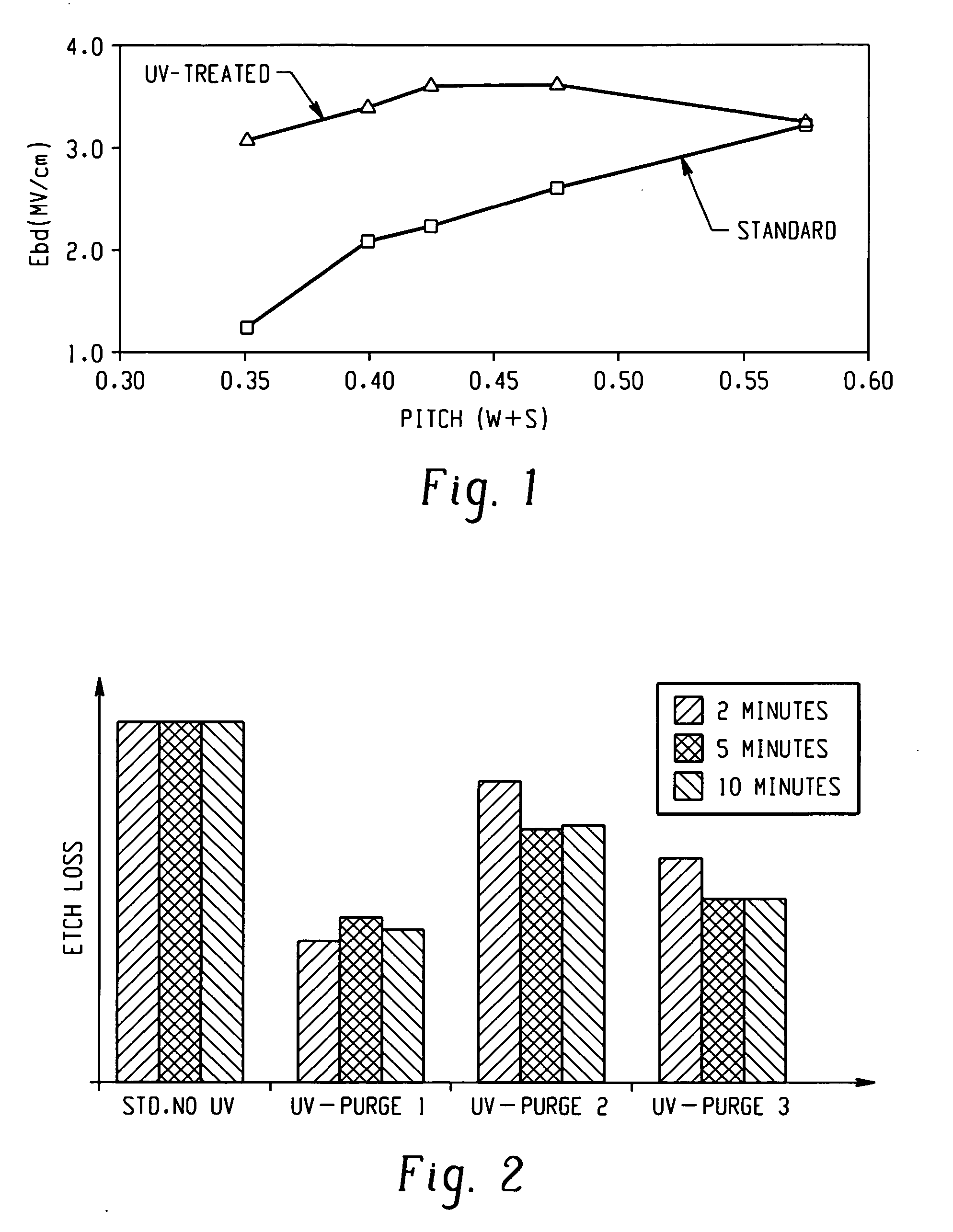
[0043] In this Example, substrates having deposited thereon a porous dielectric material were exposed to a dilute hydrofluoric acid wet etching process for different periods of time. The substrates were exposed to UV radiation in accordance with the present disclosure in an inert environment (purge-1), a reducing environment (purge-2), or an oxidizing environment (purge-3). A control was exposed to the wet etch process without any exposure to UV. The results are shown in FIG. 2, which clearly show an increase in wet etch resistance upon exposure to the UV radiation as well as a dependence on the environment in which the UV exposure occurred.


PUM

PropertyMeasurementUnit
wavelengthsaaaaaaaaaa
depthaaaaaaaaaa

Abstract

Processes for sealing porous low k dielectric film generally comprises exposing the porous surface of the porous low k dielectric film to ultraviolet (UV) radiation at intensities, times, wavelengths and in an atmosphere effective to seal the porous dielectric surface by means of carbonization, oxidation, and / or film densification. The surface of the surface of the porous low k material is sealed to a depth less than or equal to about 20 nanometers, wherein the surface is substantially free of pores after the UV exposure.

Description

BACKGROUND [0001] The present disclosure generally relates to the manufacture of semiconductor devices, and more particularly, to an ultraviolet assisted pore sealing process for porous low k dielectric materials employed in semiconductor devices. [0002] As semiconductor and other microelectronic devices progressively decrease in size, the demands placed on device components continue to increase. For example, the prevention of capacitive crosstalk between interconnect lines becomes significantly more important with smaller devices. Capacitive crosstalk is generally a function of both the distance between conductors and the dielectric constant (k) of the material placed in between the conductors. Considerable attention has been focused on electrically isolating the conductors from each other using new insulators having low dielectric constants because although silica (SiO2), which has traditionally been used in such devices because of its relatively good electrical and mechanical pro...

Claims


Application Information

Patent Timeline
Patent Type & Authority Applications(United States)
IPC IPC(8): H01L21/4763
CPCC23C16/56H01L21/02107H01L21/02203H01L21/02337H01L21/02348H01L21/31051H01L21/31058H01L21/31695H01L21/76825H01L21/76826H01L21/31H01L21/469H01L21/3105H01L21/4763
Inventor WALDFRIED, CARLOESCORCIA, ORLANDOBERRY, IVAN
Owner AXCELIS TECHNOLOGIES
Why Eureka
Try Eureka