Plasma reaction chamber and captive silicon electrode plate for processing semiconductor wafers

a technology of reaction chamber and silicon electrode plate, which is applied in the direction of electrical equipment, basic electric elements, electric discharge tubes, etc., can solve the problems of increasing the cost of using a dry plasma etching system, affecting the effect of the etching process, and prohibitively expensive showerhead electrodes that are commonly used in the industry

Inactive Publication Date: 2006-05-25
SAMSUNG AUSTIN SEMICON +1
View PDF24 Cites 32 Cited by
  • Summary
  • Abstract
  • Description
  • Claims
  • Application Information

AI Technical Summary

Problems solved by technology

The effectiveness of the etching process is greatly affected by the components of the etching chamber.
However, the showerhead electrodes that are commonly used in the industry are prohibitively expensive.
This is a consumable item that greatly increases the cost of using a dry plasma etching system.

Method used


Image

  • Plasma reaction chamber and captive silicon electrode plate for processing semiconductor wafers
  • Plasma reaction chamber and captive silicon electrode plate for processing semiconductor wafers
  • Plasma reaction chamber and captive silicon electrode plate for processing semiconductor wafers

Examples


Embodiment Construction

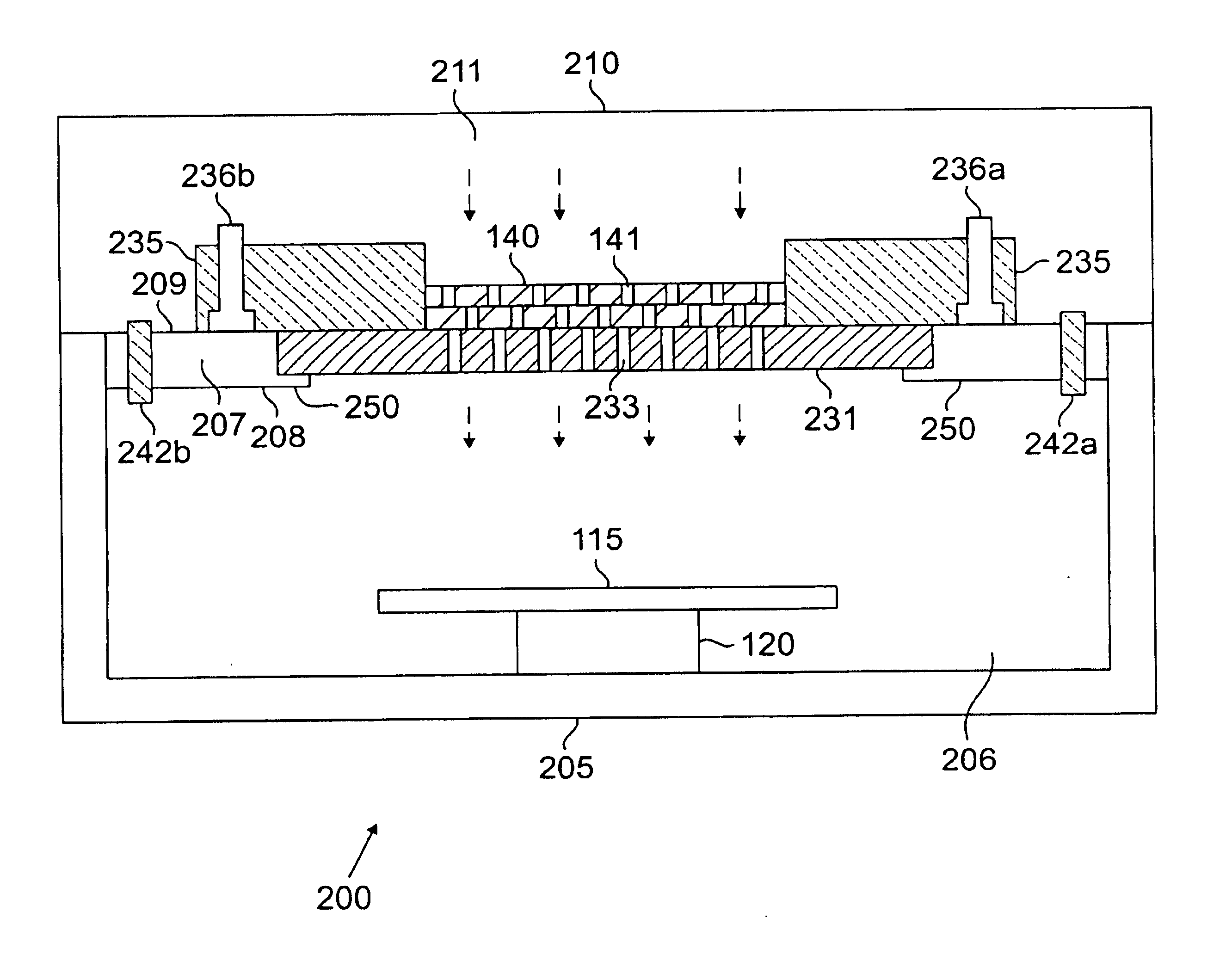
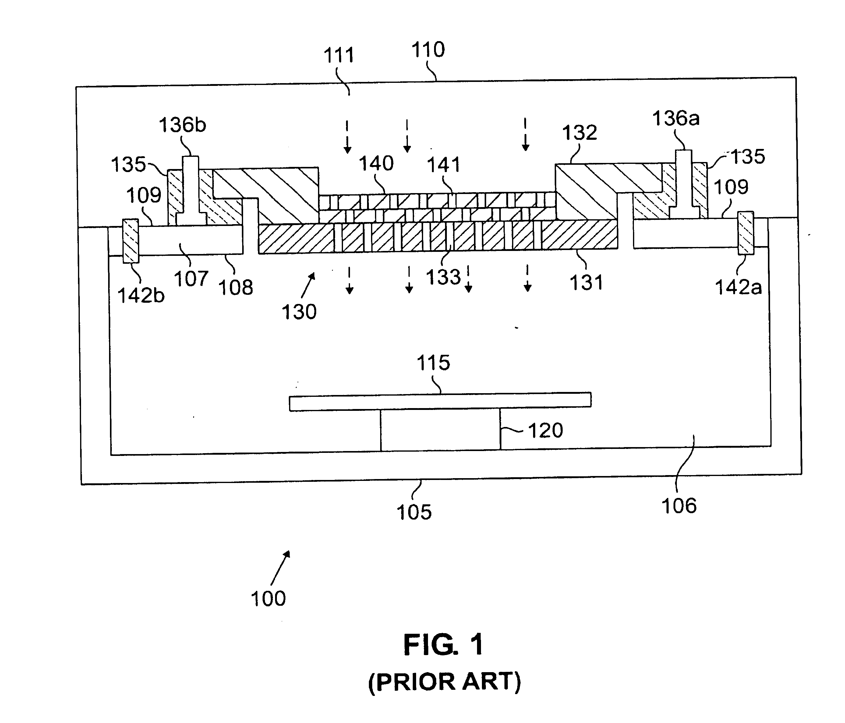
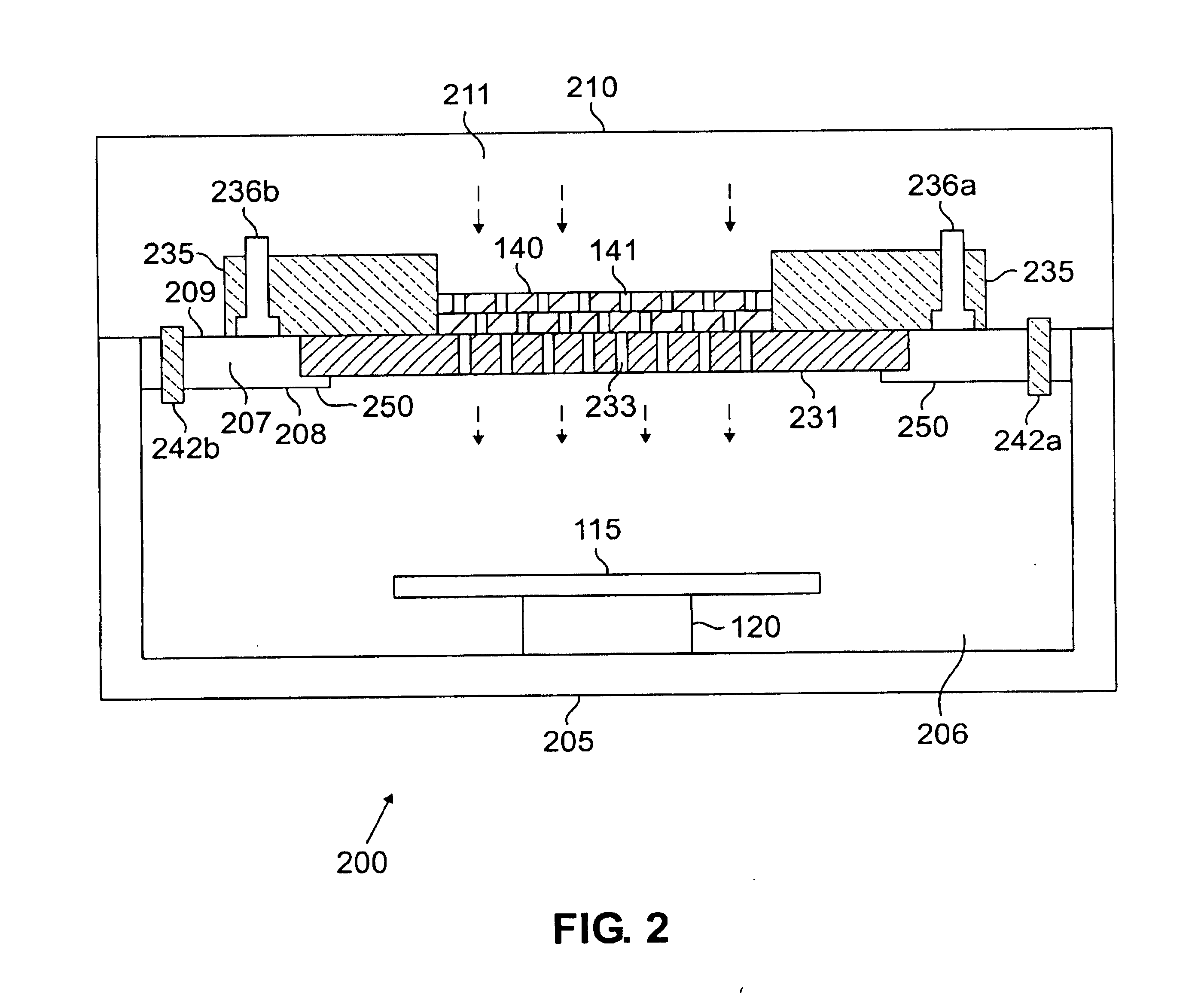
[0023]FIGS. 1 through 4, discussed below, and the various embodiments used to describe the principles of the present invention in this patent document are by way of illustration only and should not be construed in any way to limit the scope of the invention. Those skilled in the art will understand that the principles of the present invention may be implemented in any suitably arranged plasma processing system.

[0024]FIG. 1 illustrates a cross-sectional view of selected portions of conventional plasma etching system 100 according to an exemplary embodiment of the prior art. Plasma etching system 100 comprises plasma chamber 105, which encloses empty space 106. Semiconductor wafer 115 is mounted on support 120 on the bottom wall (floor) of plasma chamber 105. Plasma etching system 100 further comprises showerhead electrode assembly 130 and housing 110. Showerhead electrode assembly 130 comprises electrode plate 131 (diagonal line shading) and graphite ring 132 (lattice shading), whic...


PUM

PropertyMeasurementUnit
perimeteraaaaaaaaaa
semiconductoraaaaaaaaaa
etch rateaaaaaaaaaa

Abstract

A plasma processing system for etching a semiconductor wafer comprises: 1) a plasma chamber in which the semiconductor wafer may be mounted; 2) an upper ring capable of being mounted on an upper opening of the plasma chamber, wherein a central portion of the upper ring forms a hole; and 3) an electrode plate having a plurality of vias therethrough. The electrode plate is disposed in the hole in the upper ring, wherein the central portion of the upper ring further forms a shelf for supporting the electrode plate in the hole.

Description

TECHNICAL FIELD OF THE INVENTION [0001] The present invention generally relates to plasma processing systems and, more specifically, to a plasma reaction chamber with a captive silicon electrode for dry plasma etching of semiconductor wafers. BACKGROUND OF THE INVENTION [0002] Plasma processing techniques, such as dry plasma etching, reactive ion etching, and ion milling techniques, provide numerous advantages over traditional chemical etching of semiconductor wafers. For example, plasma etching has a vertical etch rate that is much greater than the horizontal etch rate. This provides good control over the resulting aspect ratio (i.e., the height to width ratio of the resulting notch) of the etched features. Thus, plasma etching forms very fine features with high aspect ratios in very thin films. [0003] During the plasma etching process, large amounts of energy are added to a gas at relatively low pressure, thereby ionizing the gas. This forms plasma above the masked surface of the ...

Claims


Application Information

Patent Timeline
Patent Type & Authority Applications(United States)
IPC IPC(8): C23F1/00
CPCH01J37/3244H01J37/32605H01L21/3065H01L21/67069
Inventor GERNERT, JAMES T.
Owner SAMSUNG AUSTIN SEMICON
Why Eureka
Try Eureka