

Sensor and image pickup device
- Summary
- Abstract
- Description
- Claims
- Application Information
AI Technical Summary
Benefits of technology
Problems solved by technology
Method used
Image

Examples
first embodiment
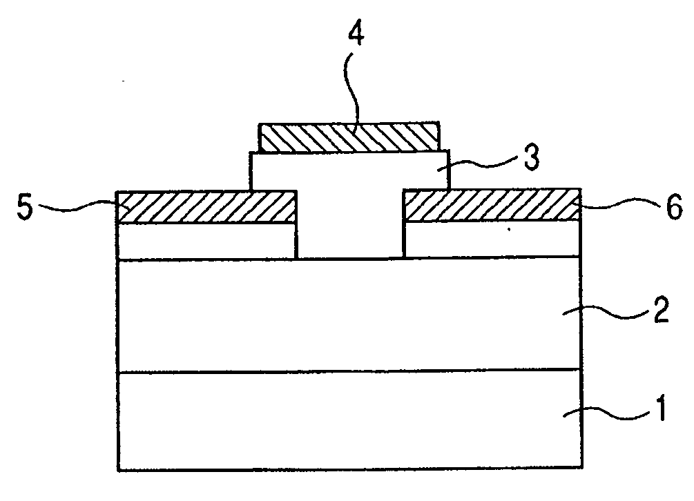
[0067]FIG. 8 shows a first schematic structural view of a sensor for detecting a received electromagnetic wave according to the present invention.
[0068] The sensor according to the present invention is constituted of a lower electrode (702), an amorphous oxide semiconductor layer (703), and an upper electrode (704) on a substrate (701).
[0069] The upper electrode may be referred to as the first electrode, and the lower electrode may be referred to as the second electrode.
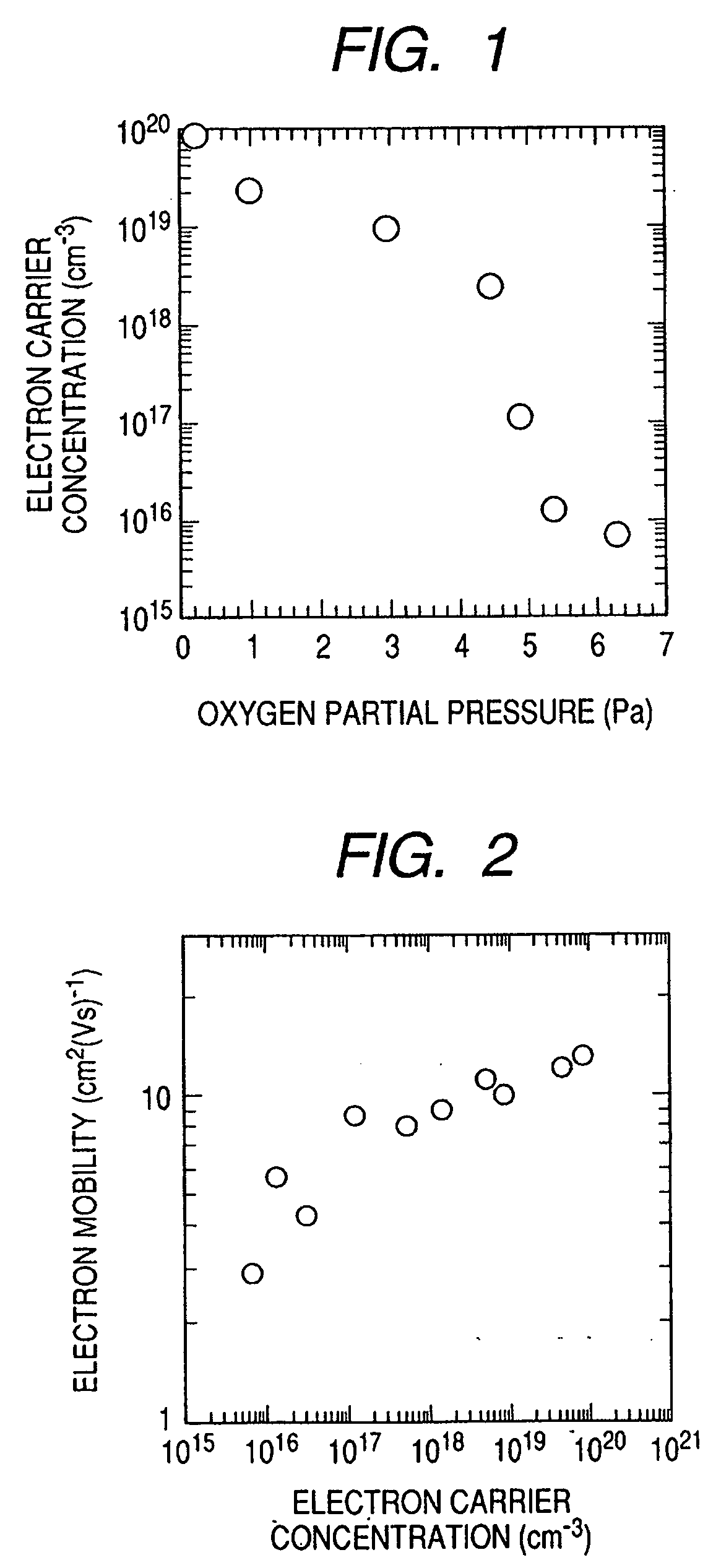
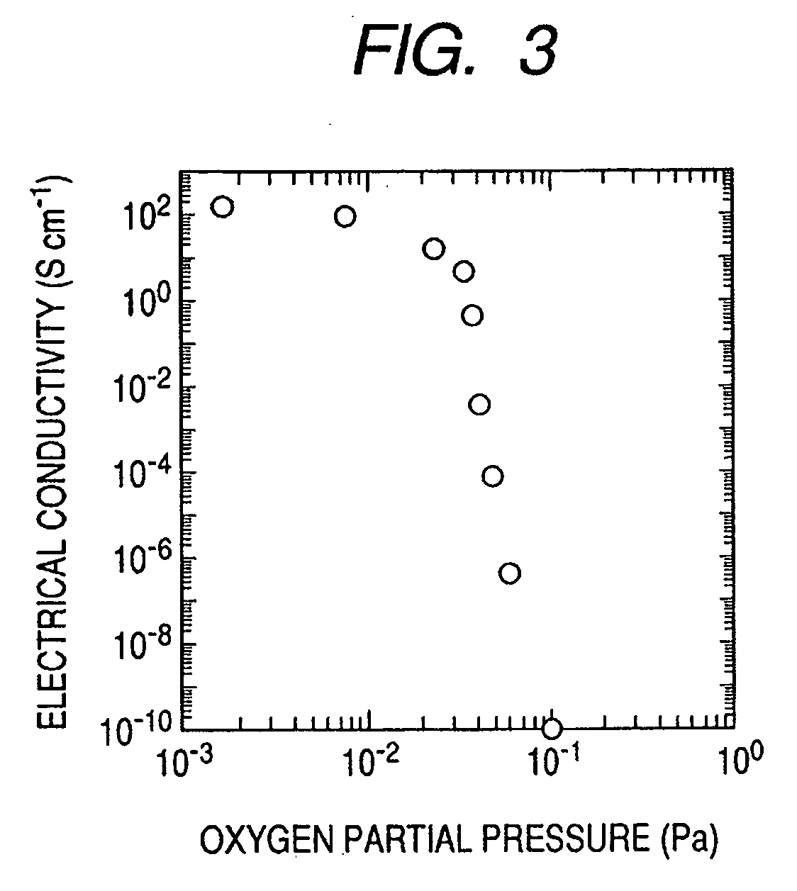
[0070] In this embodiment, for example, an oxide having an electron carrier concentration of less than 1018 / cm3 is used for the amorphous oxide layer.
[0071] The thickness of the amorphous oxide semiconductor layer, which is appropriately optimized depending on the wavelength of light with which the layer is irradiated or a pigment for pigment sensitization, is preferably 10 nm to 1 μm, or more preferably 10 nm to 500 nm.
[0072] The amorphous oxide semiconductor shows n-type conduction when it is a semiconductor c...
second embodiment
[0098]FIG. 10 shows a schematic view of an image pickup device according to the present invention. The invention according to this embodiment is, for example, an X-ray image sensor. The image pickup device of the present invention is constituted of a lower electrode 902, a semiconductor layer 903 to serve as an opto-electric conversion element, an upper electrode 904, and a scintillator 905 on a deformable substrate 901. The constitution shown in FIG. 8 or 9 can be used for the constitution from the substrate 901 to the upper electrode 904. The semiconductor layer is formed of, for example, an amorphous oxide containing at least In—Ga—Zn—O.
[0099] At least part of the image pickup device according to the present invention preferably has a non-flat portion. Of course, an image pickup device which instantaneously has a flat shape but can be deformed into a non-flat shape is also preferable.
[0100] An amorphous oxide (to be described in detail later) may be used for the semiconductor l...
example 1
[0314] An optical sensor device shown in FIG. 8 is formed. An Al electrode having a thickness of 100 nm is formed on a glass substrate (1737 manufactured by Corning Inc.) by means of a vacuum deposition method to serve as a lower electrode. Next, a polycrystalline sintered material having an InGaO3(ZnO)4 composition is used as a target to deposit an In—Ga—Zn—O-based amorphous oxide semiconductor thin film on the electrode by means of a pulse laser deposition method using a Kr excimer laser. In2O3(SnO2) having a thickness of about 20 nm is laminated on the thin film at a substrate temperature of room temperature by means of a vacuum deposition method to serve as an upper electrode. Thus, an optical sensor is formed. At the time of use, a negative bias is applied to the upper electrode on a light incidence side, and a positive bias is applied to the lower electrode. Then, the optical sensor device is irradiated with ultraviolet light having a wavelength of 365 nm from a mercury lamp. ...
PUM
 Abstract
Description
Claims
Application Information