Functional device and method for producing the same

Inactive Publication Date: 2006-05-25
FUJIFILM HLDG CORP +1
View PDF2 Cites 15 Cited by
  • Summary
  • Abstract
  • Description
  • Claims
  • Application Information

AI Technical Summary

Benefits of technology

[0039] In accordance with the invention, an insulating layer can be formed at a low temperature under proper conditions according to the constituent materials, making it possible to provide a functional device such as photoelectric conversion layer stacked type solid-state image pic

Problems solved by technology

However, with respect to the CCD type image sensor or CMOS type image sensor, the technical progress reaches the vicinity to limits, and the size of the light receiving region (opening) of one light receiving part is about 2 μm and becomes closed to the order of a wavelength of incident light, resulting in facing a problem that the production yield is poor.
Further, an upper limit of the quantity of photoelectric charges to be accumulated one miniaturized light receiving part is low as about 3,000 in terms of the number of electrons, so that it becomes difficult to express 256 gradations beautifully.
For this reason, it is difficult to ex

Method used


Image

  • Functional device and method for producing the same
  • Functional device and method for producing the same
  • Functional device and method for producing the same

Examples


Example

EXAMPLE 1

[0087] In an example of the invention, the following compounds 1 to 13 to be formed on an electrode layer to provide a photoelectric conversion layer were measured for glass transition temperature Tg by TG-DTA. Thereafter, ITO was deposited on the entire surface of a glass substrate (under the same conditions as used in the following method of depositing ITO). The aforementioned compounds were each then deposited on the glass substrate with ITO to a thickness as small as 50 nm by a resistive evaporation method to prepare 13 samples. These samples were each then determined for ΔE1 while being kept in a nitrogen atmosphere. Subsequently, ITO was deposited on each of the samples prepared under the same conditions as mentioned above (under the same deposition conditions as used in the following method of depositing ITO). These samples were each then determined for ΔE2 while being kept in a nitrogen atmosphere. From these values was then determined Tg×(ΔE2 / ΔE1 ) of the compoun...

Example

EXAMPLE 2

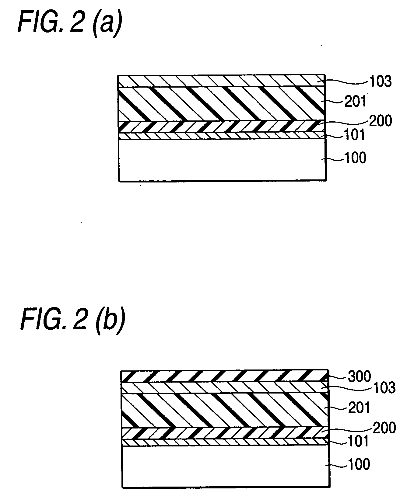
[0101] An element was prepared in the same manner as in Example 1 except that the conditions under which the organic material is deposited on the substrate which has been moved into the organic layer depositing chamber were changed as follows. In some detail, the pressure in the chamber was reduced to 3×10⁻⁴ Pa. The compound 12 was vacuum-deposited as functional layer 200 on the substrate at a rate of from 0.3 to 0.4 nm / sec to a thickness of 40 nm while the substrate holder was being rotated. A 10:1 mixture by weight of the compound 15 and the compound 16 was then deposited as functional layer 201 on the functional layer 200 to a thickness of 20 nm. The aforementioned test procedure was followed except that the compound 4 was replaced by the compounds 5, 6, 7, 9 and 10. These elements were each then measured for dark current. Thereafter, the following two insulating layers 300 (sputtering / plasma CVD) were deposited on these elements (FIG. 2(b)). During the deposition of in...


PUM


Abstract

A method of producing a functional device which comprises forming a functional layer containing an organic material, an electrode layer and an insulating layer on a substrate, wherein the step of forming the insulating layer is effected with a temperature T of the substrate being controlled to satisfy the following relationship:
T≦Tg×(ΔE2/ΔE1)
where Tg is a glass transition temperature of the organic material, ΔE1 is an activation energy for crystallization of the organic material measured while the electrode layer and the insulating layer are not stacked on the functional layer and ΔE2 is an activation energy for crystallization of the organic material while the electrode layer is formed on the functional layer.

Description

BACKGROUND OF THE INVENTION [0001] This application is based on Japanese patent application JP 2004-209903, filed on Jul. 16, 2004, the entire content of which is hereby incorporated by reference, the same as if set forth at length. [0002] 1. Field of the Invention [0003] The present invention relates a functional device and a method of producing same and more particularly to a functional device containing an organic material such as photoelectric conversion type solid-state image pickup device formed by stacking a photoelectric conversion layer containing an organic material on a substrate having a signal reading circuit formed thereon. [0004] 2. Description of the Related Art [0005] A prototype device of a photoelectric conversion layer stacked type solid-state image pickup device is, for example, one described in JP-A-58-103165. This solid-state image pickup device is constructed such that three layers of photosensitive layers are stacked on a semiconductor substrate; and respect...

Claims


Application Information

Patent Timeline
IPC IPC(8): H01L21/00
CPCH01L27/14609H01L27/14623H01L27/14647H01L27/14692H01L27/307H01L51/0058H01L51/0071H01L51/0072H01L51/0081H01L51/0085H10K39/32H10K85/626H10K85/657H10K85/6572H10K85/324H10K85/342
Inventor ARAKI, YASUSHI
Owner FUJIFILM HLDG CORP
Why Eureka
Try Eureka