Scanning probe microscope and sample observing method using this and semiconductor device production method

a scanning probe and microscope technology, applied in semiconductor/solid-state device testing/measurement, instruments, mechanical roughness/irregularity measurements, etc., can solve the problems of inability difficult to increase the speed of physically scanning the sample, etc., to achieve high-speed measurement and high precision measurement

Active Publication Date: 2006-06-01
HITACHI LTD
View PDF9 Cites 29 Cited by
  • Summary
  • Abstract
  • Description
  • Claims
  • Application Information

AI Technical Summary

Benefits of technology

[0010] Existing CD-SEM cannot cope with the problems described above. Therefore, a scanning probe microscope technology is believed promising. It is a scanning probe microscope technology capable of increasing the probe approach speed described above, less damaging a soft and brittle material and capable of acquiring information of surface materials that becomes necessary in this case.
[0011] In contrast, JP-A-11-352135 discloses a method for reducing damage of a soft and brittle material by oscillating a sample or a probe at constant amplitude and conducting scanning while the probe is allowed to periodically impinge against the sample.
[0017] In the technology described in JP-A-10-223170 described above, the apparatus becomes large in scale and damage to samples having low electron beam resistance is feared. Another problem is that the operation of monitoring the probe shape and the wear amount of the probe due to the measurement and judging the probe exchange timing or eliminating the influences on the measurement profile distortion due to the probe shape difference and the probe wear becomes an unavoidable operation for conducting highly accurately the CD measurement.
[0022] Furthermore, the invention is completed to solve the problems described above and to provide a scanning probe microscope, particularly an atomic force microscope (AFM) as one of the scanning probe microscopes, that can accurately specify and position a measurement area of a sample having a fine pattern which has been difficult to observe through an optical microscope, and can correct measurement profile distortion resulting from variance of a probe shape or probe wear on the basis of the condition of the probe shape and probe wear.
[0023] To solve the problems described above, a scanning microscope according to a first invention analyzes a sensor signal to suppress a probe retraction amount to a minimum level and uses a driving pattern for quickly completing transverse movement of a probe by using a measurement method capable of high precision measurement without damaging a sample and repeating retraction / approach of the sample, and accomplishes high speed measurement by using means for changing a control method of approach and contact of the probe.
[0025] Further, the invention accomplishes a scanning probe microscope capable of high speed approach of a probe to a sample by using a proximity sensor having high sensitivity by optical height detection.

Problems solved by technology

Various improvements have been made in the past to solve the problem inherent to the scanning probe microscope in that it is difficult to increase a speed for physically scanning the sample.
However, the technologies described above involve the problem that only a scanning probe microscope apparatus having the construction for oscillating the probe can be used and the problem that because proximity cannot be detected unless the probe approaches the sample at about several micro-meters, another sensor becomes necessary to bring at a high speed the probe to the distance of several micro-meters.
On the other hand, existing fine pattern formation processes of LSI conduct dimensional management by using CD-SEM (measuring SEM, CD: Critical Dimension) but the following problems to be solved exist with miniaturization of patterns.
Existing CD-SEM cannot cope with the problems described above.
From the aspect of the higher speed, however, high speed measurement cannot be made because retraction and approach of the probe is repeated for each measurement point.
However, when the atomic force microscope (AFM) is used for CD / sectional profile measurement in the semiconductor production lines, there are many problems to be solved such as through-put, specification and positioning of the measurement area, distortion of the measurement image resulting from scanning accuracy of an XY stage or variance of the probe shape and probe wear, and so forth.
Further, the method disclosed in JP-A-2-28113 described above involves the problem that accurate positioning of the measurement area becomes impossible in future because resolution of patterns by using the optical microscope becomes more difficult with further miniaturization of the patterns.
In the technology described in JP-A-10-223170 described above, the apparatus becomes large in scale and damage to samples having low electron beam resistance is feared.
Another problem is that the operation of monitoring the probe shape and the wear amount of the probe due to the measurement and judging the probe exchange timing or eliminating the influences on the measurement profile distortion due to the probe shape difference and the probe wear becomes an unavoidable operation for conducting highly accurately the CD measurement.
As explained above, the prior art technologies have the problems how to simultaneously satisfy the measurement not damaging the sample and the high speed measurement.

Method used


Image

  • Scanning probe microscope and sample observing method using this and semiconductor device production method
  • Scanning probe microscope and sample observing method using this and semiconductor device production method
  • Scanning probe microscope and sample observing method using this and semiconductor device production method

Examples


Embodiment Construction

[0071] Hereinafter, the invention will be explained by using the drawings.

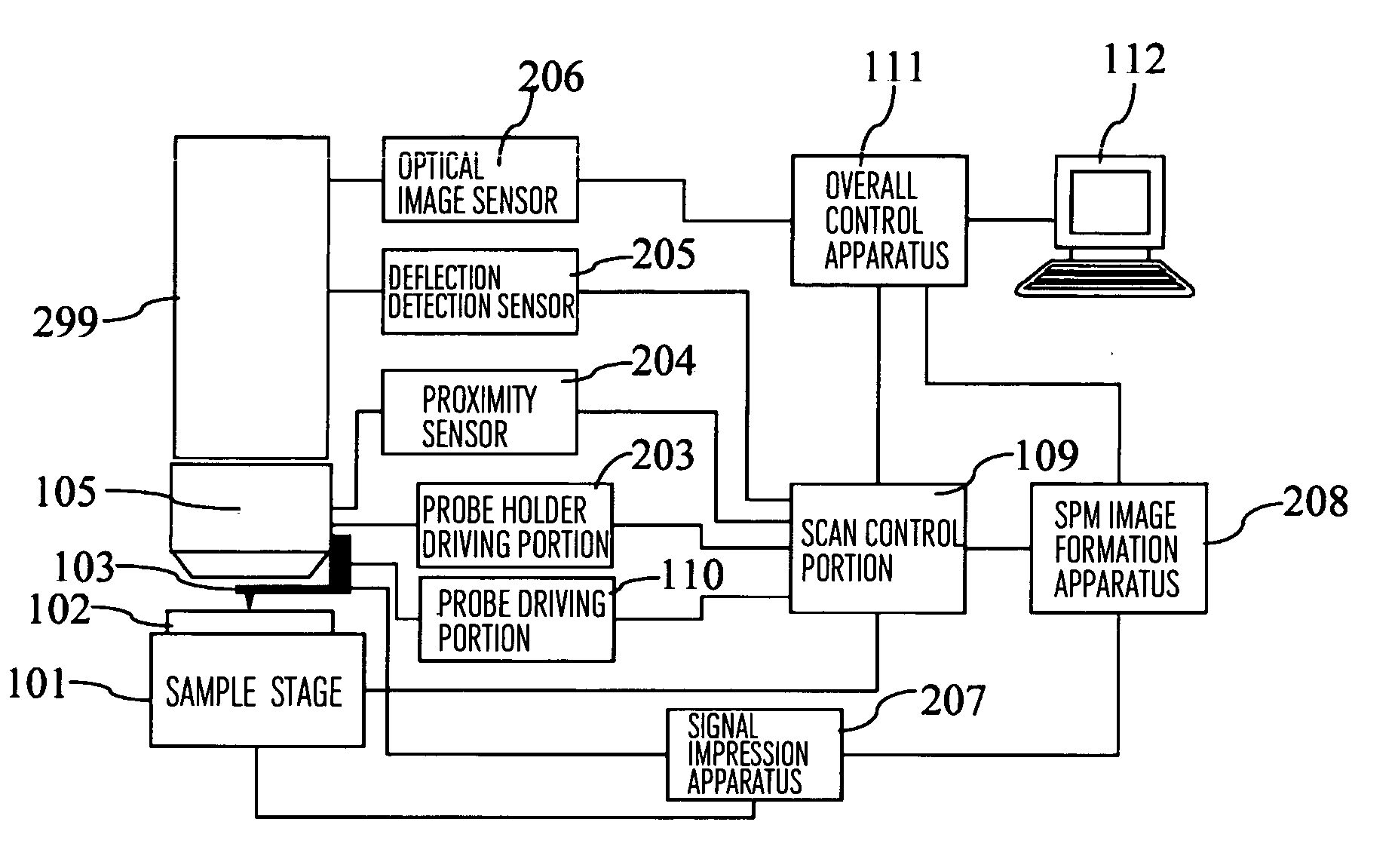
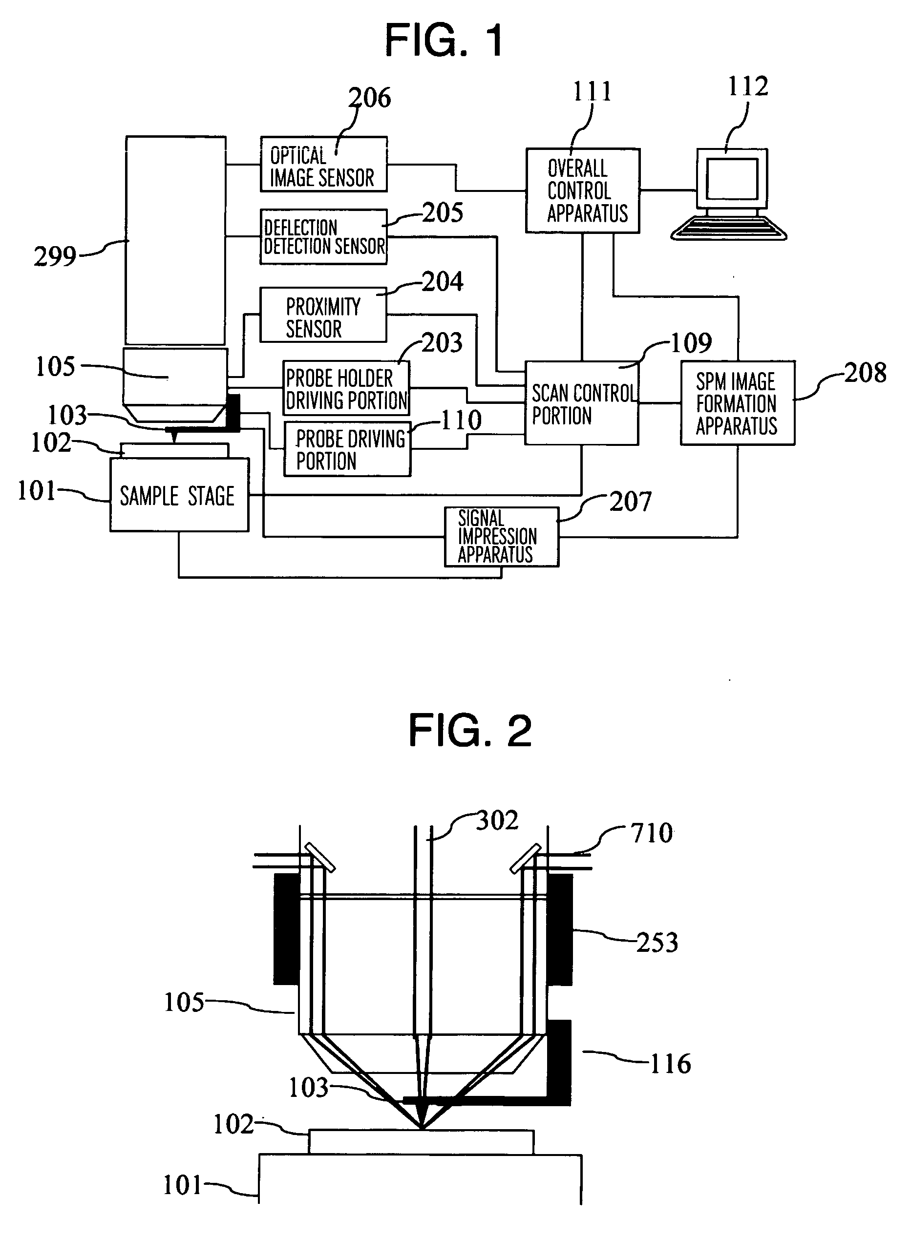
[0072]FIG. 1 is a view showing a construction of a scanning probe microscope according to the invention. FIG. 2 is an enlarged view of a portion around a probe in an embodiment. A sample 102 is put on a sample stage 101 that can be driven in X, Y and Z directions. The sample stage is controlled by a scanning control portion 109. A probe 103 exists above the scan control portion 109. A probe moving mechanism 116 to which the probe 103 is fitted is driven by control from a probe driving portion 110 in the X, Y and Z directions and conducts probe scanning of the scanning probe microscope.

[0073] The probe moving mechanism 116 is fitted to a probe holder 105. The probe holder 105 is fitted to a barrel 299 by a probe holder up / down mechanism 253 and is roughly driven and moved in the Z direction under control from a probe holder driving portion 203. A probe moving mechanism 116 is a fine movement mechanism and doe...


PUM


Abstract

A scanning probe microscope capable of measuring accurate 3-D shape information of a sample with high through-put without damaging a sample. In a method for acquiring an accurate 3-D shape of a sample without imparting damage to the sample by bringing a probe into contact at only a measurement point, once pulling up and retracting the probe when it moves towards a next measurement point, moving the probe towards the next measurement point and allowing it to approach, a deflection signal of the probe and its twist signal area analyzed so that measurement can be made at a minimum necessary retraction distance. Control for minimizing residual oscillation at the time of transverse movement is made so that a measurement frequency can be raised and high speed measurement can be accomplished.

Description

TECHNICAL FIELD [0001] This invention relates to a scanning probe microscope technology, a sample observation method using this and a device / optical recording media production method. More particularly, the invention relates to a technology that will be effective when it is applied to specification of a measurement area and correction of the measurement result. BACKGROUND ART [0002] A scanning probe microscope (SPM) is known as a measuring technology of fine three-dimensional shapes. This is a technology that scans a sample while a probe whose tip is pointed is controlled and contact force is kept at an extremely small value, and has widely been employed as a technology capable of measuring fine three-dimensional shapes in an atomic order. Various improvements have been made in the past to solve the problem inherent to the scanning probe microscope in that it is difficult to increase a speed for physically scanning the sample. [0003] For example, JP-A-10-142240 and JP-A-2000-162115 ...

Claims


Application Information

Patent Timeline
Patent Type & Authority Applications(United States)
IPC IPC(8): G21K7/00G01B21/30G01Q10/02G01Q30/02G01Q30/06G01Q40/02G01Q60/18G01Q60/24G01Q60/38H01L21/66
CPCB82Y35/00G01Q10/06G01Q10/065G01Q30/06G01Q20/04G01Q30/025G01Q20/02
Inventor BABA, SHUICHINAKATA, TOSHIHIKOWATANABE, MASAHIROARAI, TAKESHI
Owner HITACHI LTD
Why Eureka
Try Eureka