
Probe look ahead: testing parts not currently under a probehead

a technology of probeheads and probes, applied in the direction of semiconductor/solid-state device testing/measurement, basic electric elements, instruments, etc., can solve the problems of significant portion of the overall manufacturing cost of such devices, time and equipment needed for testing memory devices, and high cost of ics testing, so as to reduce or eliminate the need for burn-in stress, reduce costs and problems, and save time and equipmen

Inactive Publication Date: 2006-06-01
MICRON TECH INC
View PDF31 Cites 11 Cited by
  • Summary
  • Abstract
  • Description
  • Claims
  • Application Information

AI Technical Summary

Benefits of technology

The present invention provides a semiconductor substrate with a metal layer for re-routing power and signals to testing pads on a semiconductor die. The substrate also includes look-ahead contacts that are electrically connected to the testing pads on the die to allow for stressing or testing of the die. The invention also provides a probe card for testing the dies on the substrate and a method for testing the dies on the substrate using the probe card. The technical effects of the invention include improved testing and stressing of dies on a semiconductor substrate.

Problems solved by technology

Testing of ICs is expensive and time consuming, and it is desirable to keep testing costs low since these add directly to the cost of producing the parts.
Because each memory cell or bit of the memory device must be tested, the time and equipment necessary for testing memory devices represents a significant portion of the overall manufacturing cost of such devices.

Method used


Image

  • Probe look ahead: testing parts not currently under a probehead
  • Probe look ahead: testing parts not currently under a probehead
  • Probe look ahead: testing parts not currently under a probehead

Examples


Embodiment Construction

[0039] The invention will be described generally with reference to the drawings for the purpose of illustrating embodiments only and not for purposes of limiting the same. The figures illustrate processing steps for use in fabricating semiconductor devices in accordance with the present invention. It should be readily apparent that the processing steps are only a portion of the entire fabrication process.

[0040] In the current application, the terms “semiconductive wafer fragment” or “wafer fragment” or “wafer” will be understood to mean any construction comprising semiconductor material, including but not limited to bulk semiconductive materials such as a semiconductor wafer (either alone or in assemblies comprising other materials thereon), and semiconductive material layers (either alone or in assemblies comprising other materials). The term “substrate” refers to any supporting structure including, but not limited to, the semiconductive wafer fragments or wafers described above. ...


PUM


Abstract

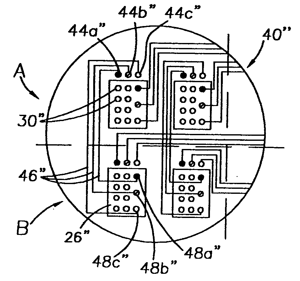
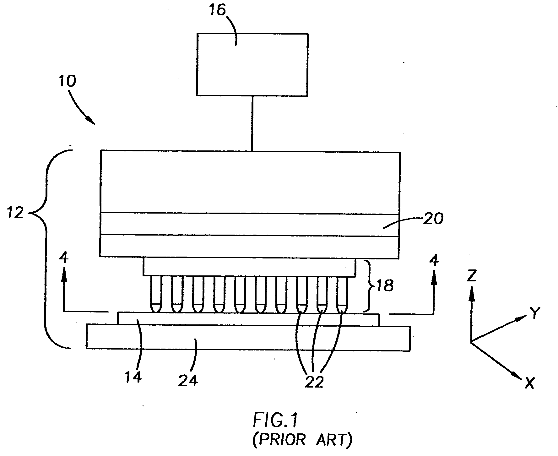
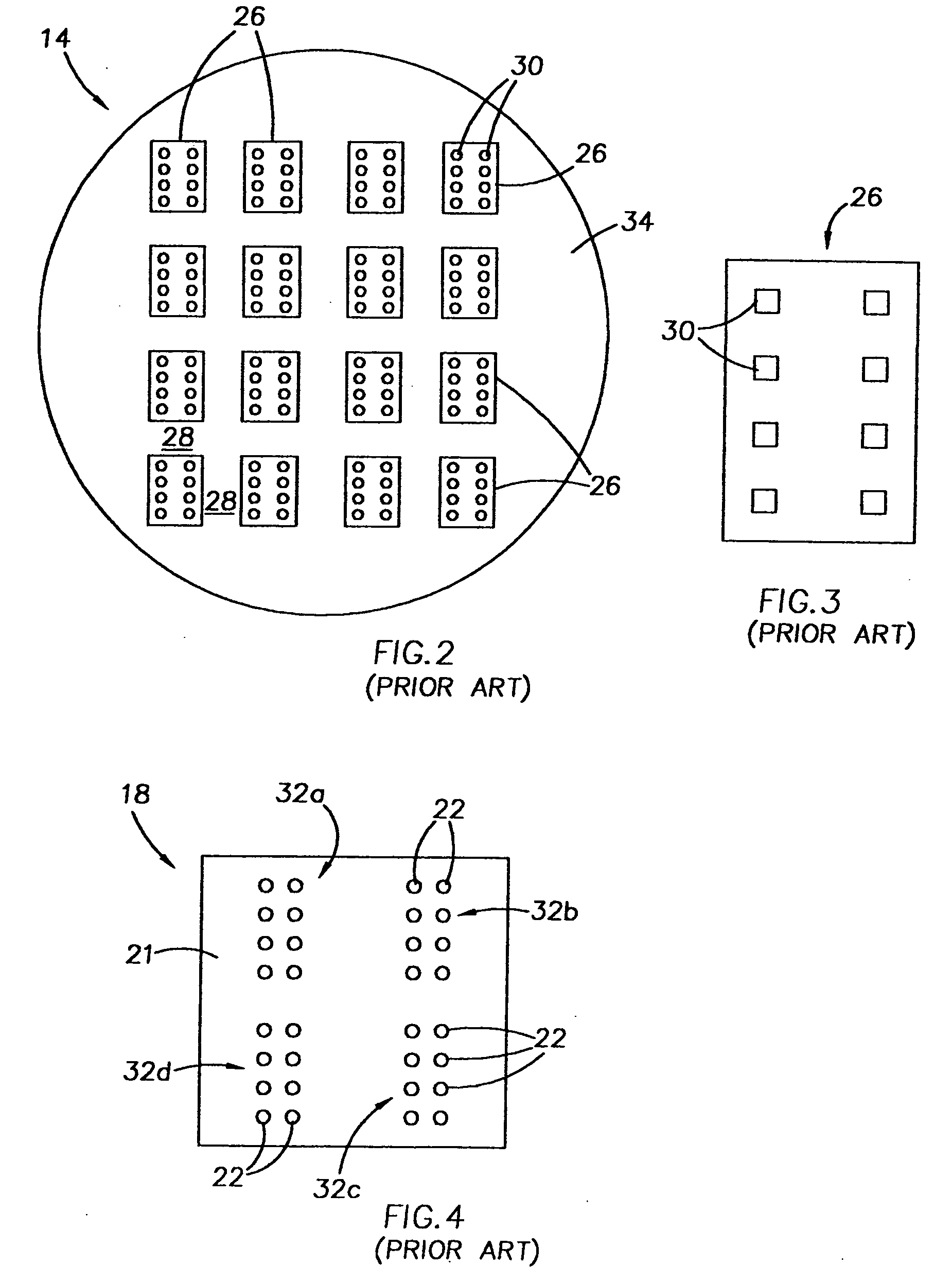
A semiconductor substrate, probe card, and methods for stressing and testing dies on a semiconductor substrate are provided. The semiconductor substrate, typically a semiconductor wafer, comprises dies disposed thereon and a redistribution layer (RDL) for routing signals from a test circuit into dies on the substrate that are not currently under probe. The RDL includes look-ahead contacts associated with a first die set that are electrically connected by traces to dies of a second die set. Upon contact of elements of the probe tester with the look-ahead contacts, required Vcc power, GND ground potential and signals from the probe tester are routed through the traces to the die of the die set not currently under probe. The dies can comprise a built-in self-stress (BISS) circuit and / or a built-in self-test (BIST) circuit for implementing a stress or test sequence. The look-ahead contacts allow for overlapping or substantially simultaneously stressing and / or testing dies of dies of a die set currently under probe and dies of a second die set located prior to or after the current probe head position (i.e., not under probe).

Description

CROSS-REFERENCE TO RELATED APPLICATIONS [0001] This application is a divisional of U.S. Ser. No. 10 / 654,655, filed Sep. 3, 2003, pending, which is a divisional of U.S. Ser. No. 10 / 178,111, filed Jun. 24, 2002, now U.S. Pat. No. 6,630,685.FIELD OF THE INVENTION [0002] This invention relates to testing of semiconductor dies disposed on a semiconductor substrate. BACKGROUND OF THE INVENTION [0003] After a semiconductor wafer has been fabricated, a number of the dies on the wafer are inoperable. Manufacturers of semiconductor devices typically test the individual dies for functionality prior to singulation into individual dies, to evaluate various electrical parameters of the integrated circuit components contained on each die, and verify that certain standards are met. Integrated circuits (IC) devices typically undergo three separate test cycles: (1) in-process testing and monitoring of sheet resistivities, junction depths, and device parameters such as current gain and voltage breakdo...

Claims


Application Information

Patent Timeline
Patent Type & Authority Applications(United States)
IPC IPC(8): H01L23/58H01L23/34G01R31/28G11C5/02G11C7/00H01L23/544
CPCG01R31/2831G01R31/2884G11C29/006G11C29/06G11C29/56G11C2029/5602H01L22/32H01L22/34
Inventor LUNDE, ARON T.
Owner MICRON TECH INC
Learn More