Method and apparatus for polymer dielectric surface recovery by ion implantation

a technology of ion implantation and dielectric surface, which is applied in the direction of electrical equipment, semiconductor devices, semiconductor/solid-state device details, etc., can solve the problems of depleting or degrading some of the very properties of the polymer used, adversely affecting the dielectric constant of the polymer, and steps implemented during vlsi fabrication

Inactive Publication Date: 2006-06-01
TAIWAN SEMICON MFG CO LTD
View PDF17 Cites 8 Cited by
  • Summary
  • Abstract
  • Description
  • Claims
  • Application Information

AI Technical Summary

Problems solved by technology

Thermal curing can adversely affect the dielectric constant of the polymer.
The processing steps implemented during the VLSI fabrication can also deplete or degrade some of the very properties for which the polymer is used.
The pretreatment steps can damage the dielectric propert...

Method used


Image

  • Method and apparatus for polymer dielectric surface recovery by ion implantation
  • Method and apparatus for polymer dielectric surface recovery by ion implantation
  • Method and apparatus for polymer dielectric surface recovery by ion implantation

Examples


Embodiment Construction

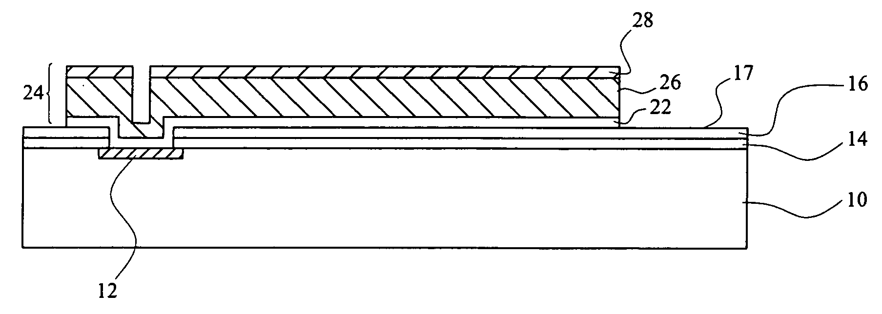
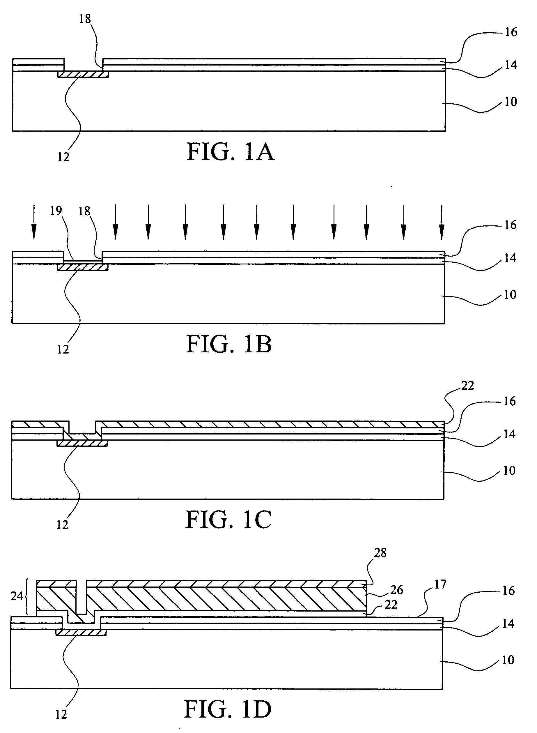
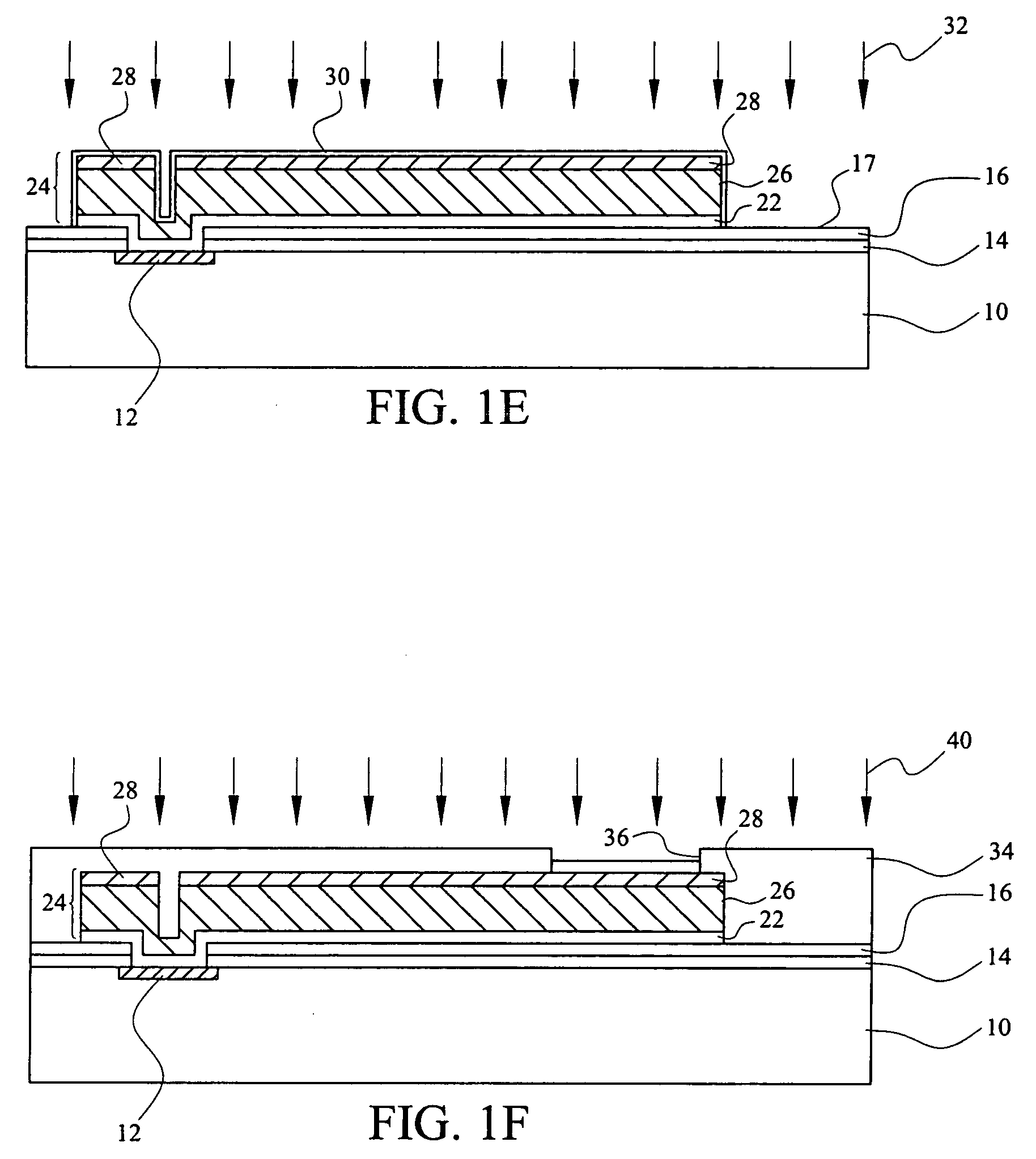
[0010] Among semiconductor-processing techniques, ion implantation is unique in that process parameters, such as concentration and depth of the desired dopant can be specified directly in the equipment settings to deliver a desired implant dose and energy. Ion implantation is advantageous over the chemical vapor deposition and other conventional deposition methods since parameters such as film thickness and density can be more accurately controlled. Conventional ion implantation process is a method by which ions of a material can be implanted into another solid to change the physical attributes of the solid. Ion implantation can impart a chemical and a structural change in the target. A chemical change can be the result of introducing a different element than the target's own composition. The structural change occurs because the crystal structure of the target can be damaged or even destroyed.

[0011] A typical ion implantation equipment can include an ionization chamber, an accelara...


PUM


Abstract

In one embodiment, the disclosure relates to a method and apparatus for surface recovery of a polymer insulation layer through implantation. The method includes providing a substrate having thereon a conductive pad and an insulation layer, optionally processing the conductive pad to remove oxide layer formed on the conductive pad and conducting ion implantation to recover dielectric properties of the insulation layer.

Description

BACKGROUND [0001] Fabrication of microelectronics devices makes effective use of patterned microelectronics conductor layers employed as interconnections for signal and power propagation by separating such conductor layers by means of blanket and / or patterned dielectric layers. Advances in speed and performance requirements, along with decreases in dimensions have made the requirements placed upon such dielectric layers more stringent with respect to lowering the “relative dielectric constants” of the dielectric layers (i.e., the dielectric constants relative to vacuum). The “relative dielectric constant” of a dielectric layer is hereinafter referred to for brevity as the “dielectric constant” of the dielectric layer. Dielectric layers having a lower dielectric constant are typically disposed between and around patterned microelectronics conductor layers during the fabrication process. Such dielectric layers reduce parasitic capacitance and cross-talk. [0002] Due to the availability...

Claims


Application Information

Patent Timeline
IPC IPC(8): H01L23/58
CPCH01L23/3114H01L2224/0401H01L24/12H01L2224/0231H01L2224/13099H01L2224/16H01L2924/01013H01L2924/01018H01L2924/01022H01L2924/01029H01L2924/01075H01L2924/12044H01L2924/14H01L2924/30105H01L2924/01006H01L2924/01024H01L2924/01033H01L2924/014H01L24/11H01L24/02H01L24/03H01L24/05H01L24/13H01L2224/05124H01L2224/05147H01L2224/05155H01L2224/05166H01L2224/05171H01L2224/05548H01L2224/05647H01L2224/13024H01L2924/0001H01L2924/00014H01L2224/02H01L2924/01028H01L2924/013
Inventor YU, HSIU-MEICHOU, KEN-SHENHSU, SHUN-LIANG
Owner TAIWAN SEMICON MFG CO LTD
Why Eureka
Try Eureka