Methods for assembling a stack package for high density integrated circuits

a technology of integrated circuits and stack packages, applied in the direction of printed circuit components, printed circuit testing/measurement, semiconductor/solid-state device testing/measurement, etc., can solve the problem that software applications require enormous amounts of volatile random access memory (ram) at increasingly high speeds, and achieve the effect of reducing the size of the pcb

Inactive Publication Date: 2006-06-01
KYOCERA CORP
View PDF16 Cites 22 Cited by
  • Summary
  • Abstract
  • Description
  • Claims
  • Application Information

AI Technical Summary

Benefits of technology

[0005] The present invention provides stack packages for high density application specific integrated circuits (ASIC's) and memory modules that effectively reduce PCB size. A PCB usually contains a plurality of layers, the densest of which is the interconnection betwe

Problems solved by technology

Additionally, these electronic connections are often manufactured to be as dense as possible such that they use the least possible amount of space on the

Method used


Image

  • Methods for assembling a stack package for high density integrated circuits
  • Methods for assembling a stack package for high density integrated circuits
  • Methods for assembling a stack package for high density integrated circuits

Examples


Embodiment Construction

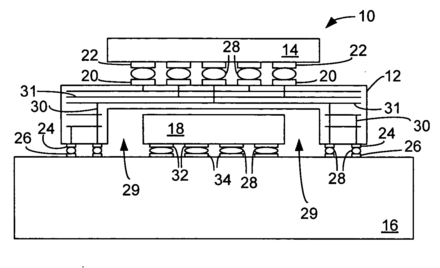
[0022] Referring to FIG. 1, a stack package 10 for a high density IC module will now be described. Stack package 10 comprises an interposer 12, an IC 14 and a chip carrier 18 in electrical communication with a PCB 16. IC 14 may be an ASIC, such as a wireless communication signal base band processor. Chip carrier 18 may be a memory chip carrier 18. For purposes of illustration, IC 14 is discussed herein as an ASIC and chip carrier 18 is discussed as a memory chip carrier 18. The packaging and connecting methods and systems described herein can be used with other types of IC's and chips, such as, for example, general microprocessors and peripheral integrated circuits associated with ASIC's and microprocessors, such as digital signal processor, wireless communication transmit and receive chips. Additionally, many types of memory are possible, as will be described more fully below.

[0023] As seen in FIG. 1, memory chip carrier 18 is directly mounted on the PCB 16 and interposer 12 is di...


PUM


Abstract

Methods for assembling a stack package for a high density IC module on a PCB include the steps of assembling a first layer of the stack package on the PCB, assembling a second layer of the stack package on the first layer and assembling a third layer of the stack package on the second layer, such that each layer is provided in electrical communication with the PCB. Additional layers may be added to the stack package.

Description

CROSS REFERENCE TO RELATED APPLICATIONS [0001] This application is a continuation-in-part of U.S. patent application Ser. No. 11 / 002,480, filed Dec. 1, 2004, the contents of which are incorporated herein by reference in their entirety.FIELD OF THE INVENTION [0002] The present invention relates generally to systems and methods for assembling integrated circuit (IC) stack packages. BACKGROUND OF THE INVENTION [0003] Electronic package designs for today's high speed electronic systems (e.g., computers, cell phones, network devices, etc.) must provide quality electrical performance and reliable electronic connections between various system components such as cards, chips, boards, modules, etc. Additionally, these electronic connections are often manufactured to be as dense as possible such that they use the least possible amount of space on the printed circuit board (PCB). [0004] Most modern software applications require enormous amounts of volatile random access memory (RAM) at increas...

Claims


Application Information

Patent Timeline
IPC IPC(8): H01L21/50
CPCH01L22/34H01L23/5385H01L24/16H01L24/48H01L25/0657H01L25/50H01L2224/32145H01L2224/48227H01L2225/0651H01L2225/06513H01L2225/06517H01L2225/06541H01L2225/06572H01L2225/06596H01L2924/15153H01L2924/15311H01L2924/15321H01L2924/3511H05K1/0284H05K1/141H05K1/182H05K3/3436H05K2201/041H05K2201/09072H05K2201/10378H05K2201/10515H05K2201/10674H05K2201/10734H05K2203/1572H01L2924/01087H01L2224/0554H01L2224/05568H01L2224/05573H01L2924/00014H01L2924/14H01L2924/00H01L2224/05599H01L2224/45099H01L2224/45015H01L2924/207H01L2224/0555H01L2224/0556
Inventor NGUYEN, CAM T.ZHU, SHERRY XIAOQI
Owner KYOCERA CORP
Why Eureka
Try Eureka