
Surface-activation of semiconductor nanostructures for biological applications

Inactive Publication Date: 2006-06-01
SPIRE
View PDF11 Cites 11 Cited by
  • Summary
  • Abstract
  • Description
  • Claims
  • Application Information

AI Technical Summary

Benefits of technology

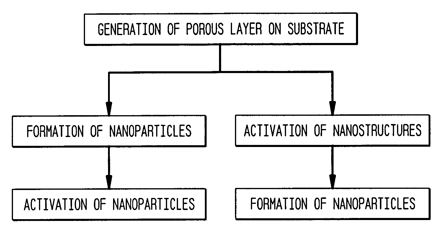
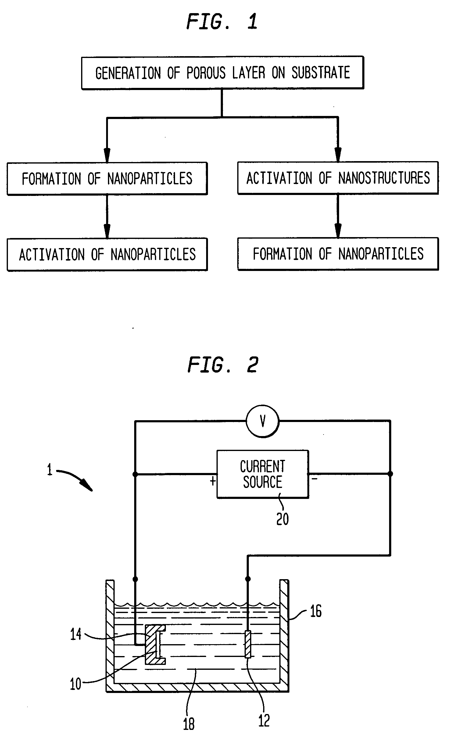
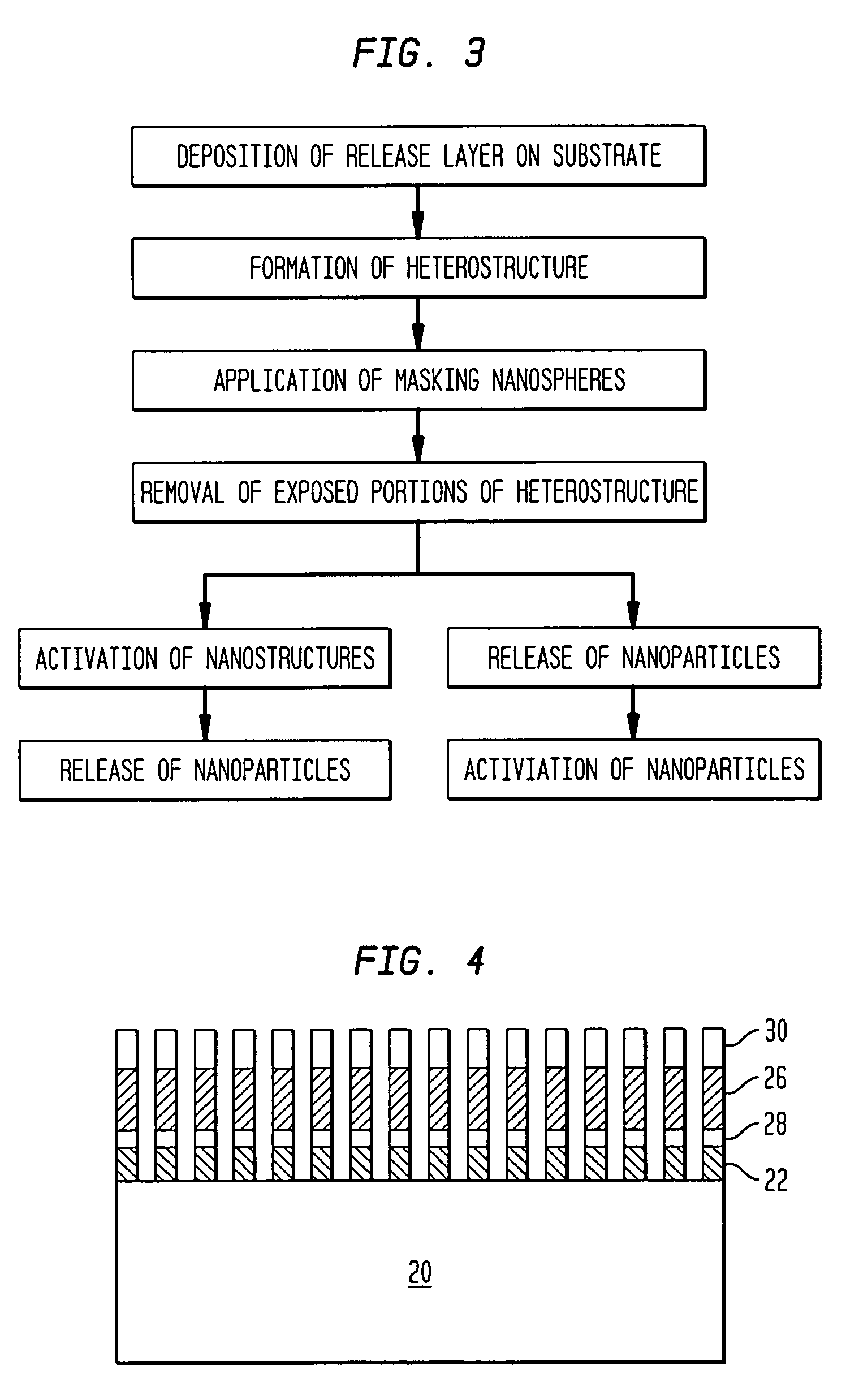
[0009] In another aspect, semiconductor nanoparticles can be produced by (1) depositing a release layer on a semiconductor substrate; (2) forming a heterostructure over the release layer; (3) applying a plurality of masking nanoparticles to portions of the surface of the heterostructure such that part of the surface of the heterostructure can be selectively etched; (4) removing the exposed portion of the heterostructures wherein a plurality of nanostructures are formed attached to the release layer; (5) activating at least a portion of a surface of the nanostructures to enhance their hydrophilicity; and (6) dissolving the release layer whereby semiconductor nanoparticles are formed. The nanostructures can be activated by exposure to an ECR plasma, oxidation or ion implantation, and the activation step can also occur after the release layer is dissolved and the semiconductor nanoparticles are formed.

Problems solved by technology

While organic fluorophores have had some success, they tend to be unstable and gradually degrade when exposed to blue or UV excitation light, in a phenomenon known as photobleaching, or simply degrade with time.
Further, such molecules typically emit light in the normal visible region, similar to that of other materials used in biological applications, resulting in a poor signal to noise ratio.
Organic fluorophores that emit light in the near-infrared region are not generally commercially available and, hence, difficult to obtain.
Because such inorganic materials can be toxic when used in vivo, a coating of a protective material usually is necessary to render them useful in biological applications.
However, as a result of the coating, which absorbs and / or reflects light, the fluorescent properties of the material are diminished.
Moreover, many inorganic nanostructures are hydrophobic by nature and consequently are not easily dissolved or suspended in aqueous solutions, rendering their use difficult in various applications, both in vitro and in vivo.

Method used


Image

  • Surface-activation of semiconductor nanostructures for biological applications
  • Surface-activation of semiconductor nanostructures for biological applications
  • Surface-activation of semiconductor nanostructures for biological applications

Examples


Embodiment Construction

[0015] In one aspect, the present invention provides methods for producing surface-activated semiconductor nanoparticles suitable for in vitro and in vivo applications which can fluoresce in response to light excitation. The terms “quantum dots,”“nanostructures” and “nanoparticles” are used interchangeably herein to describe compositions on the order of less than a nanometer to a few micrometers in size, and more preferably from about 1 to about 100 nanometers of active device structure, that possess optical properties derived from excitation of a confined population of charge carriers.

[0016] The semiconductor nanostructures of the present invention can be activated in various ways, such as by exposing their surfaces to a plasma, oxidation or ion bombardment. Once the surface is activated, functionalization of the nanoparticle for either in vitro or in vivo use can occur.

[0017] So that the invention is more clearly defined, “activated” semiconductor nanostructures or “activated” s...


PUM


Abstract

The present invention provides means and methods for producing surface-activated semiconductor nanoparticles suitable for in vitro and in vivo applications that can fluoresce in response to light excitation. Semiconductor nanostructures can be produced by generating a porous layer in semiconductor substrate comprising a network of nanostructures. Prior or subsequent to cleavage from the substrate, the nanostructures can be activated by an activation means such as exposing their surfaces to a plasma, oxidation or ion implantation. In some embodiments, the surface activation renders the nanostructures more hydrophilic, thereby facilitating functionalization of the nanoparticles for either in vitro or in vivo use.

Description

FIELD OF THE INVENTION [0001] This application relates to the production of semiconductor nanoparticles, and in particular to the production of surface-activated biocompatible semiconductor nanoparticles. BACKGROUND OF THE INVENTION [0002] Semiconductor nanoparticles, or quantum dots, are nanometer or micrometer-sized semiconductor structures in which one to a few thousand charge carriers, e.g., electrons, are confined, giving them a unique ability to emit visible or near infrared (IR) photons within a very narrow spectrum and with high efficiency. Because of this, semiconductor nanoparticles can be useful in numerous biological, genomic and proteomic applications, for example, as markers, as components of microchip arrays (biochips), and as conjugates for fluoroimmunoassays for in vitro and in vivo molecular imaging studies. [0003] At present, fluorophores synthesized from organic molecules typically are used in such applications. While organic fluorophores have had some success, t...

Claims


Application Information

Patent Timeline
IPC IPC(8): H01L21/26
CPCB82Y10/00G01N21/6489Y10S977/773Y10S438/96Y10S977/786Y10S977/888Y10S977/774
Inventor KALKHORAN, NADER M.MOE, JAMES G.LINDEN, KURT J.SAMBITO, MARISA
Owner SPIRE
Learn More