Normally closed zero insertion force connector

a technology of zero insertion force and connector, which is applied in the direction of coupling contact members, coupling device connections, electrical apparatus construction details, etc., can solve the problems of stressing components, soldering these connectors to printed circuit boards, and increased scrutiny of tin lead alloy solder and associated chemicals, so as to reduce stress

Inactive Publication Date: 2006-06-01
R&D SOCKETS INC
View PDF51 Cites 35 Cited by
  • Summary
  • Abstract
  • Description
  • Claims
  • Application Information

AI Technical Summary

Benefits of technology

[0018] The present normally closed connector provides a natural coupling and decoupling between devices, the connector housing, and a PCB. Movement of the contact members corrects for lack of co-planarity, provides shock and vibration dampening, and reduces stress at the interface. The housing and contact member geometry and material are designed primarily to provide the desired deflection mechanism, rather than contact retention. The contact members allow for compression of both contact tips approximately at the same time. The achievable pitch is l

Problems solved by technology

High reliability for such connections is essential due to potential system failure caused by improper connections of devices.
The tin lead alloy solder and associated chemicals used throughout the process of soldering these connectors to the printed circuit board have come under increased scrutiny due to their environmental impact.
The plastic housings of these connectors undergo a significant amount of thermal activity during the soldering process, which stresses the component and threatens reliability.
The soldered contacts on the connector body are typically the mechanical support for the device being interfaced by the connector and are subject to fatigue, stress deformation, solder bridging, and co-planarity errors, potentially causing premature failure or loss of continuity.
In particular, as the mating connector or semiconductor device is inserted and removed from the connector attached to th

Method used


Image

  • Normally closed zero insertion force connector
  • Normally closed zero insertion force connector
  • Normally closed zero insertion force connector

Examples


Embodiment Construction

[0035] The present invention relates to an alternate mechanism and method for actuating an LGA socket such that the contact tips are not exposed to damage prior to insertion of the LGA device. The actuating device can also control the force applied by the contact members on the LGA device.

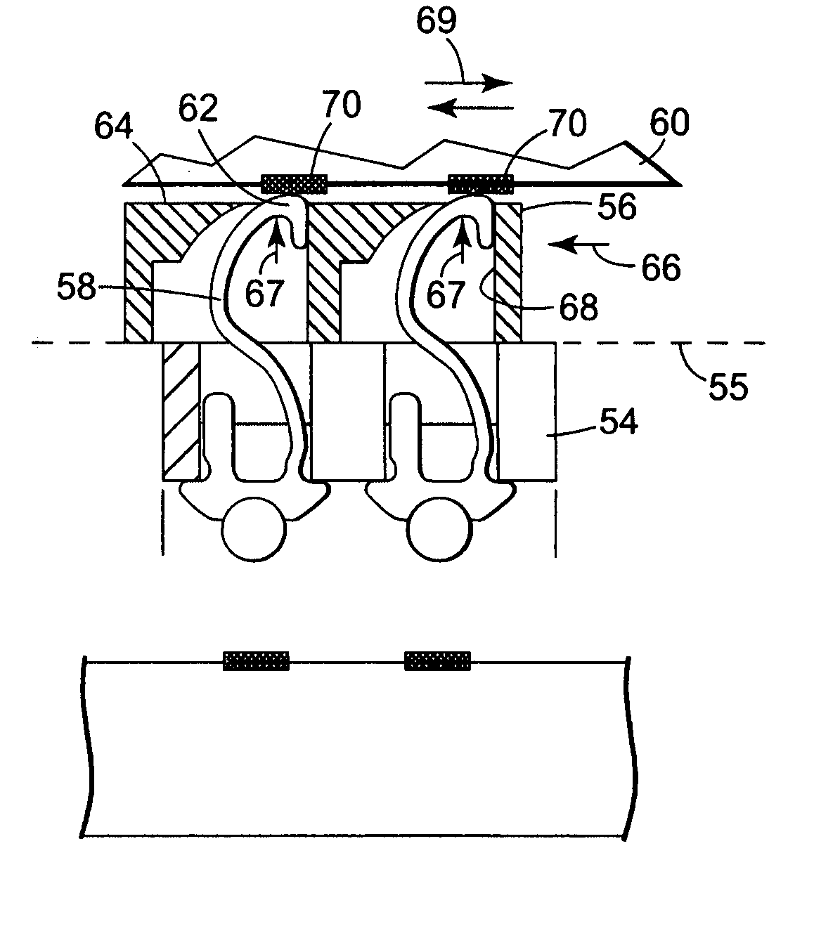
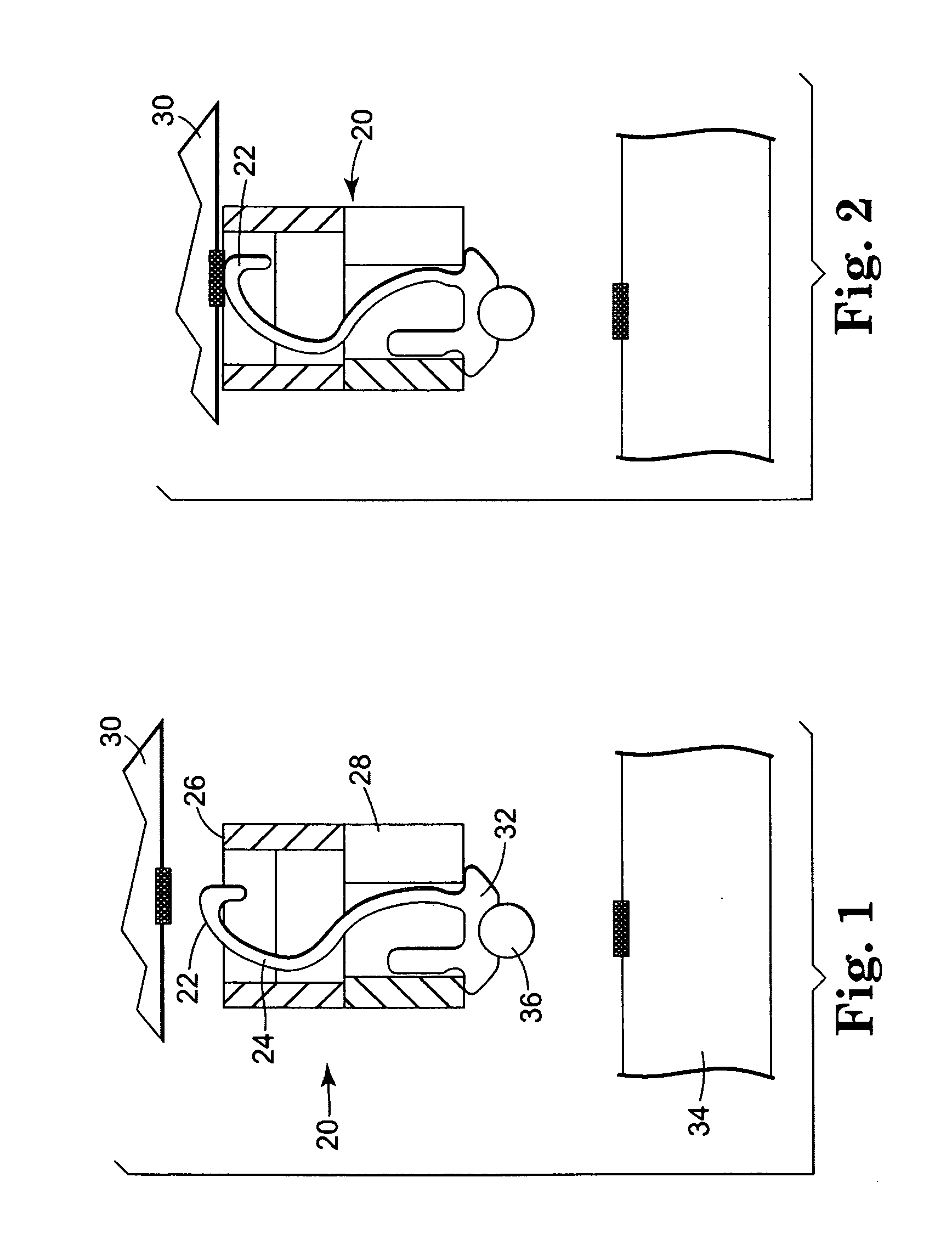
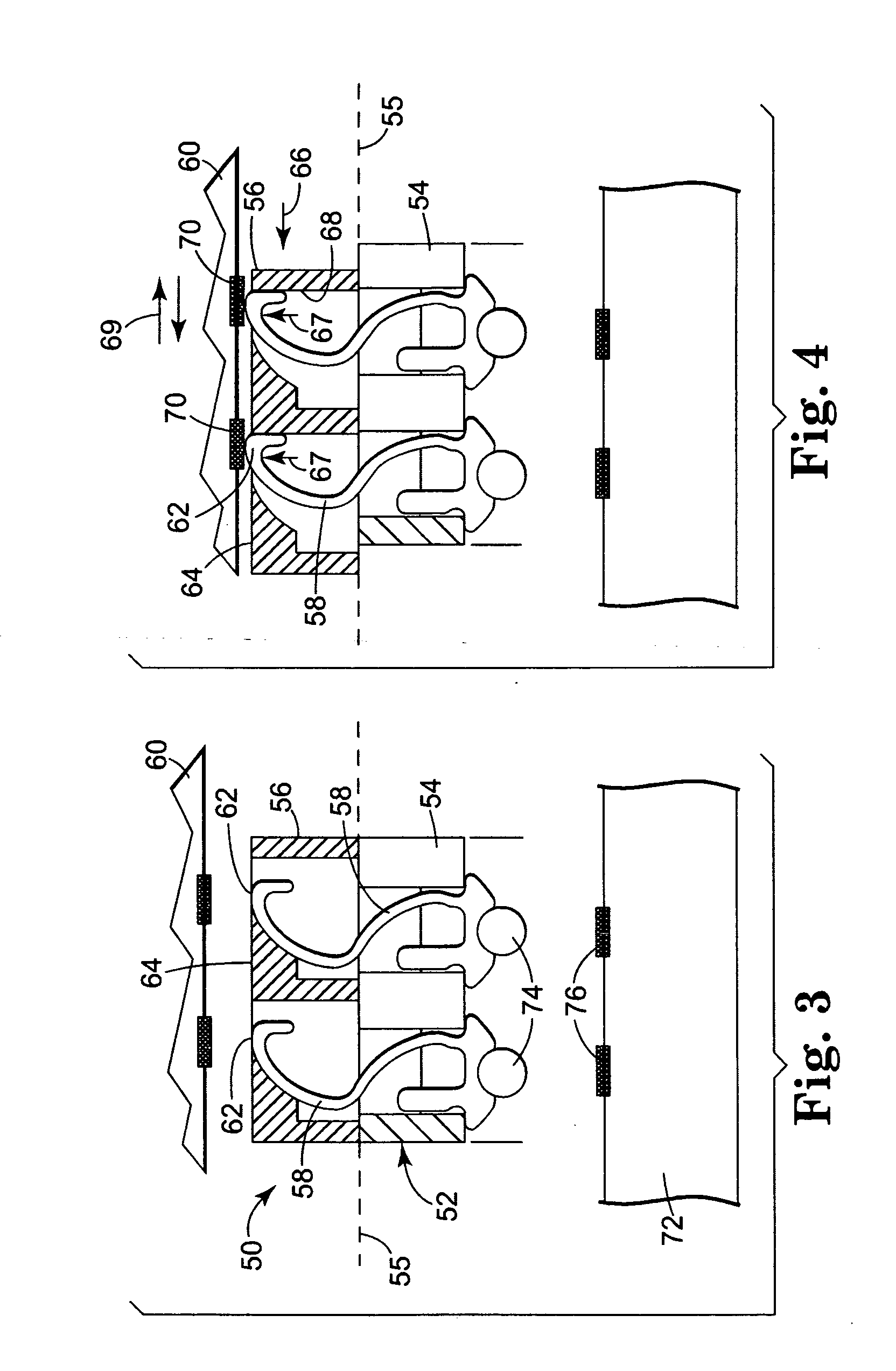
[0036] As illustrated in FIGS. 3 and 4, the connector 50 includes a housing 52 with a first portion 54 and a second portion 56. In the illustrated embodiment, the first portion 54 is stationary and retains contact members 58. The contact members 58 are preferably stamped or formed. The contact members 58 can be retained in the first portion 54 of the housing 52 by press fitting, insert molding, encapsulating, stitching, and a variety of other techniques. Various configurations of contact members and methods of encapsulating such contact members are disclosed in U.S. Pat. Nos. 5,913,687; 5,938,451; 6,135,783; 6,178,629; 6,231,353; 6,247,938 and 6,409,521, all issued to Rathburn. Although only two c...


PUM


Abstract

A normally closed connector apparatus for electrically connecting first and second circuit members. An electrically insulative connector housing having a first portion translatable relative to a second portion is provided. The connector housing is adapted to be positioned substantially between the first and second circuit members. A plurality of resilient contact members are retained in the first portion of the housing. The contact members have first distal ends that do not extend substantially above an upper surface of the second portion. Displacement of the second portion relative to the first portion in a translated configuration positions the first distal ends of the contact members above the upper surface of the second portion to electrically couple with the first circuit member.

Description

[0001] The present application is a continuation of prior application no. PCT / US2004 / 021292 entitled Normally Closed Zero Insertion Force Connector, filed Jul. 1, 2004, which claims the benefit of U.S. Provisional Patent application Ser. No. 60 / 485,508, entitled Normally Closed Zero Insertion Force Connector, filed Jul. 7, 2003, the complete disclosure of which are hereby incorporated by reference.FIELD OF THE INVENTION [0002] The present invention is directed to a normally closed, zero insertion force connector and to a replaceable chip module utilizing the present connector for electrically connecting one or more first circuit members to a second circuit member. BACKGROUND OF THE INVENTION [0003] The current trend in connector design for those connectors utilized in the computer field is to provide both high density and high reliability connectors between various circuit devices. High reliability for such connections is essential due to potential system failure caused by improper ...

Claims


Application Information

Patent Timeline
IPC IPC(8): H01R12/00H01L23/48H01R12/16H01R13/193H01R13/24H05K7/10
CPCH01R13/193H01R13/2435H01R13/2442H01R43/0249H05K7/1069H01L2924/0002H01R12/714H01R12/85H01L2924/00
Inventor RATHBURN, JAMES J.
Owner R&D SOCKETS INC
Why Eureka
Try Eureka