Lateral PNP transistor and the method of manufacturing the same

a technology of pnp transistor and lateral pnp, which is applied in the direction of basic electric elements, semiconductor devices, electrical equipment, etc., can solve the problems of complex circuit design, increase process complexity, increase the number of masks, and cost, and achieve accurate control of the width of the base and the collector, improve the performance of products, and eliminate the mismatch of multiple alignments

Inactive Publication Date: 2006-06-08
BCD SEMICON MFG
View PDF11 Cites 9 Cited by
  • Summary
  • Abstract
  • Description
  • Claims
  • Application Information

AI Technical Summary

Benefits of technology

[0011] Additional purpose of this invention is to enhance the performance of products by using LPNP without special and complicated circuit design.
[0012] Further, this invention uses a composite mask to do multiple diffusions by self-alignment. Thus, the mismatch of multiple alignments could be eliminated and the width of base and collector could be controlled accurately.
[0015] According to the defined method as described above, self-alignment process is proceeded to eliminate the misalignment between multi layers. Thus, the current gain (Hfe) of LPNP transistor can be optimized and accurately controlled by the doping concentration and depth of N-type base and P+ emitter which diffused by two times through the same doping window. Also, the collector-base breakdown voltage (BVceo) can be optimized and accurately controlled by the distance between collector window and emitter window which formed in one time, and P− collector doping concentration and depth.

Problems solved by technology

Generally there is no good PNP transistor in most bipolar processes, because this process generally is designed to make the best performance of vertical NPN transistor.
Although the vertical PNP may be added into the manufacturing process, it will increase the process complexity, number of mask, and cost.
Owing to the limitations of LPNP performance, either big area LPNP or complicated circuit design will be needed to satisfy the request of the product.

Method used


Image

  • Lateral PNP transistor and the method of manufacturing the same
  • Lateral PNP transistor and the method of manufacturing the same
  • Lateral PNP transistor and the method of manufacturing the same

Examples


Embodiment Construction

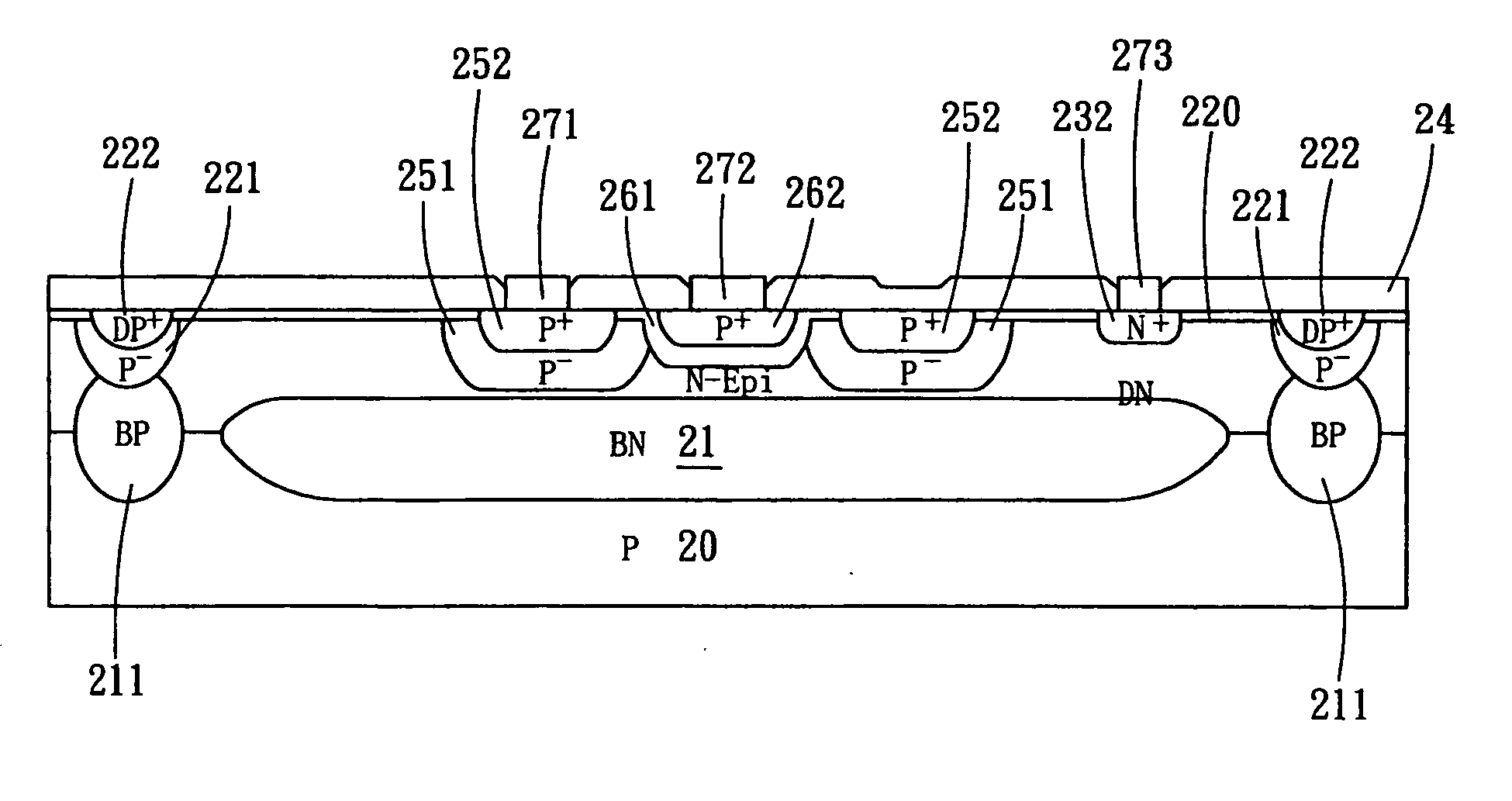
[0023] Referring to FIGS. 2-10, the descriptions of these figures are shown as below:

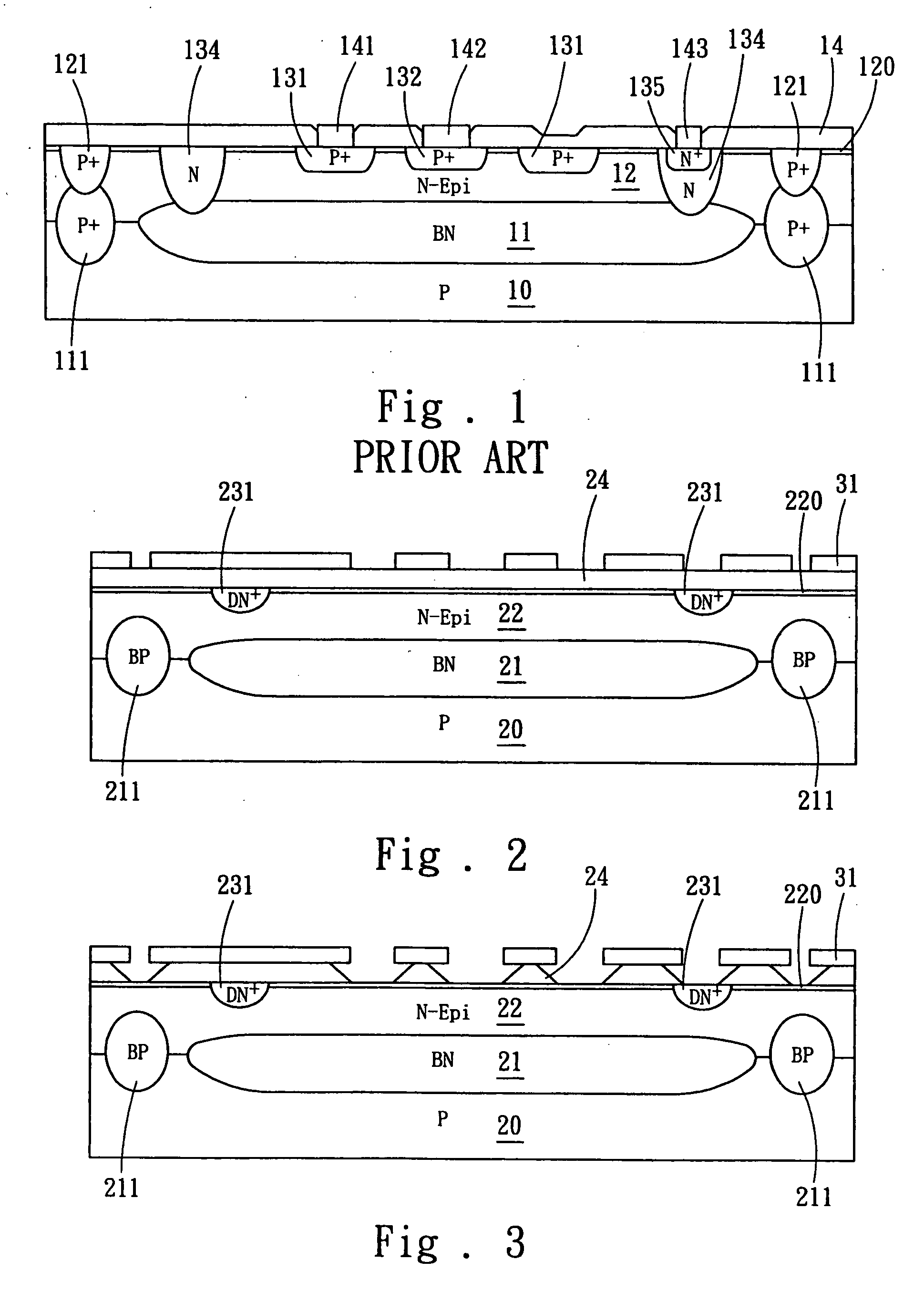
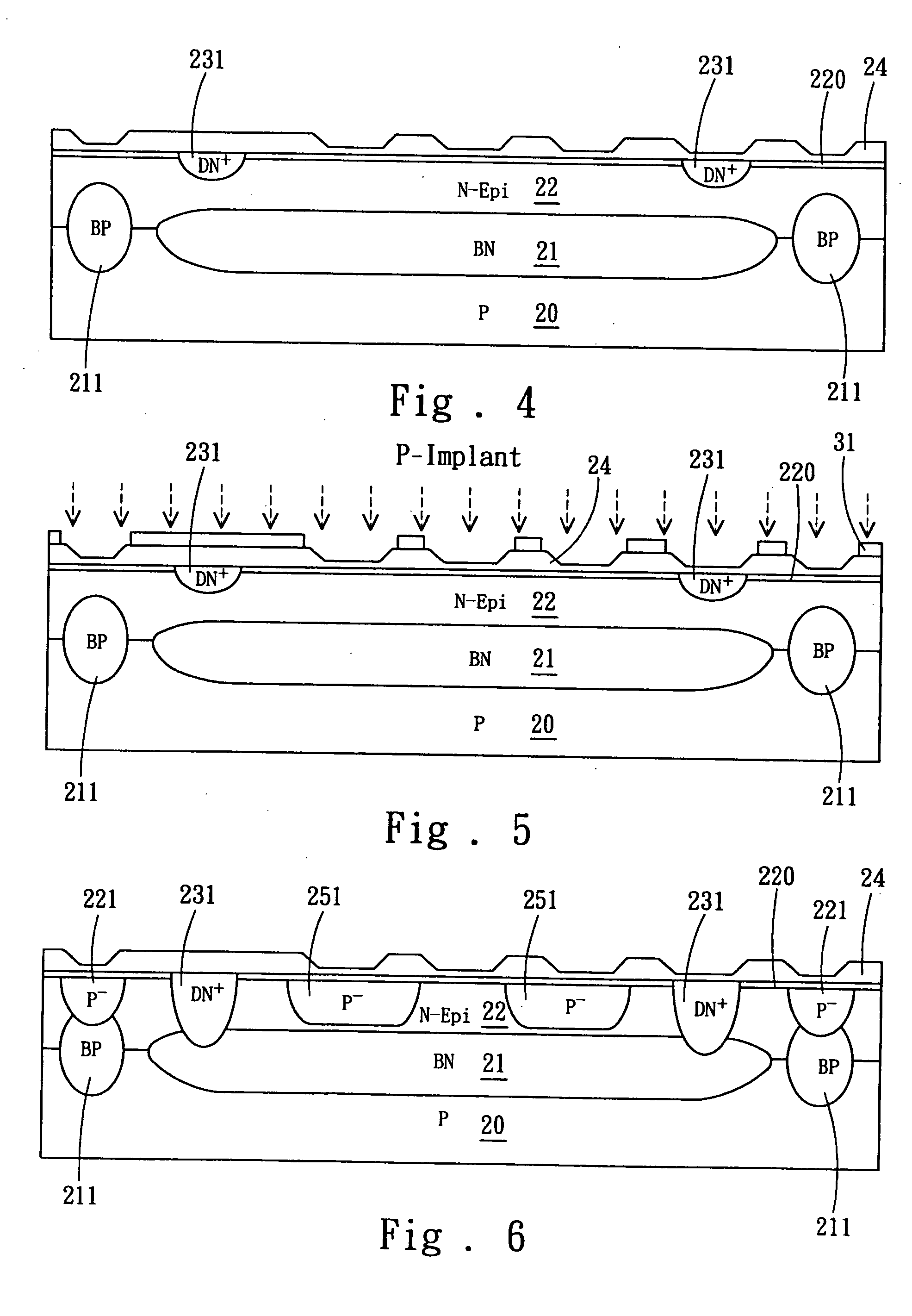
[0024] Referring now to the FIG. 2, an N-type buried layer 21, which is made by N-type implant and drive-in, is formed on the surface of P-type doping substrate 20. These layers all formed according to well-known semiconductor processing techniques. The P-type buried layers 211, which is made by P-type implant and drive-in processes, surround around the N-type buried layer 21. Next, the N-type epi layer 22 and N-type field implant layer 220 are formed sequentially on the surface of substrate 20, N-type buried layer 21, and P-type buried layers 211. Furthermore, the deep N+-type sinker areas, which are made by photolithography, etch, and N+-sinker doping processes downward the surface of field implant layer 220, formed on top of the buried layer 21. Next, the oxide layer 24 is formed on the N-type field implant layer 220. Finally, the resist mask layers 31, which define the regions of LPNP transisto...


PUM


Abstract

The present invention relates to a lateral PNP transistor and the method of manufacturing the same. The medium doping N-type base area and the light doping P− collector area were first introduced in the structure before the formation of P+ doping emitter area and the collector area. The emitter-base-collector doping profile in the lateral and the base width of LPNP were similar to NPN. The designer can optimize the doping profile and area size of each area according to the request of the current gain (Hfe), collector-base breakdown voltage (BVceo), and early voltage (VA) of LPNP transistor. These advantages may cause to reduce the area and enhance performance of the LPNP transistor.

Description

[0001] This application is a Divisional of co-pending application Ser. No. 10 / 930,851, filed on Sep. 1, 2004, and for which priority is claimed under 35 U.S.C. § 120; the entire contents of all are hereby incorporated by reference.FIELD OF THE INVENTION [0002] This invention is related to a lateral PNP transistor and the method of manufacturing the same. The invented lateral PNP transistor is mainly aimed at power driver and power output application to reduce the chip area and enhance the performance of products. BACKGROUND OF THE INVENTION [0003] The common tendency of microelectronic circuit is to integrate more functions on the chip in order to increase the widely applications of electric circuit, reduce the size and power consumption of system, and lower the price of devices. Although the bipolar transistor and bipolar process technology do not suit all applications, they are some key foundations for other extended process technology, like BiCMOS and BiCDMOS, for a long time. [0...

Claims


Application Information

Patent Timeline
Patent Type & Authority Applications(United States)
IPC IPC(8): H01L29/76
CPCH01L21/8249H01L29/6625H01L29/735
Inventor REN, CHONGLIU, XIAN-FENGQIU, BIN
Owner BCD SEMICON MFG
Why Eureka
Try Eureka